Production method for novel piezoelectric thin-film resonator

A piezoelectric thin film and resonator technology, applied in the field of preparation of new piezoelectric thin film resonators, can solve the problems of complex preparation process and high manufacturing cost, and achieve the effects of simplified process, strong mechanical properties and stable resonance area

Inactive Publication Date: 2009-08-05
SHANGHAI UNIV OF ENG SCI
View PDF0 Cites 11 Cited by
  • Summary
  • Abstract
  • Description
  • Claims
  • Application Information

AI Technical Summary

Problems solved by technology

But at present, the preparation process of this kind of piezoelectric thin film resonator is quite complic

Method used


Image

  • Production method for novel piezoelectric thin-film resonator
  • Production method for novel piezoelectric thin-film resonator
  • Production method for novel piezoelectric thin-film resonator

Examples


Embodiment approach

[0020] Embodiment: prepare piezoelectric thin film resonator, its steps are:

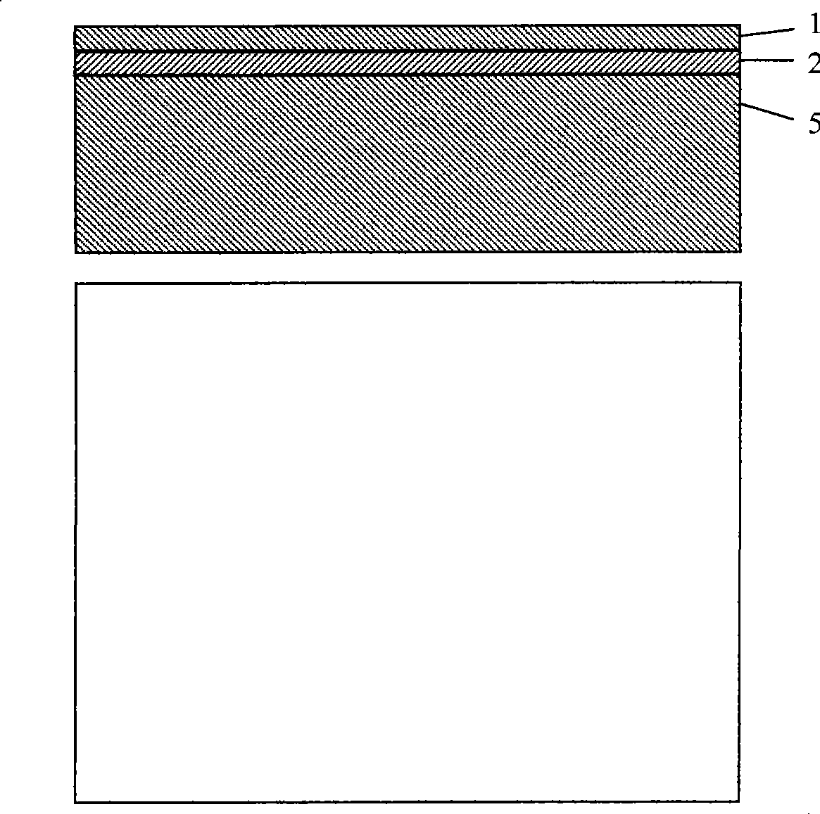
[0021] (1), substrate cleaning: take SOI wafer as substrate (see figure 1 ), put it into a mixture of hydrogen peroxide, ammonia and deionized water (the ratio is 1:3:10) and boil for 3 minutes, then put it into a mixture of hydrogen peroxide, hydrochloric acid and deionized water (the ratio is 2:3:10) for 3 minutes, soaked in a mixture of hydrofluoric acid and deionized water (1:10) for a few seconds, and finally dried with nitrogen.

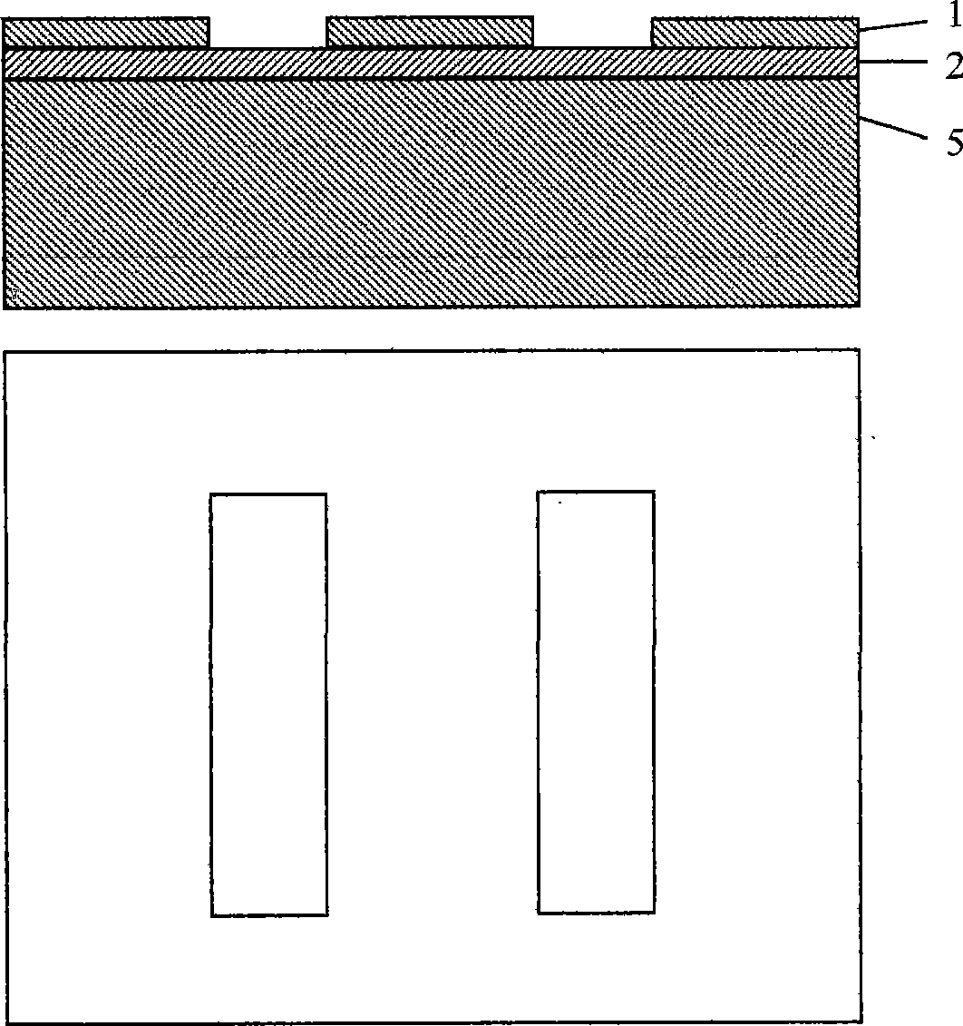
[0022] (2), photolithography of the top layer silicon etching groove: adopt the method of coating photoresist, after exposure, development, and finally corrode the unprotected part of photoresist, the window of top layer silicon is etched and formed (see figure 2 ). The etchant used is nitric acid (HNO 3 ), hydrofluoric acid (HF), acetic acid (CH 3 COOH) and deionized water in several proportions mixed solution.

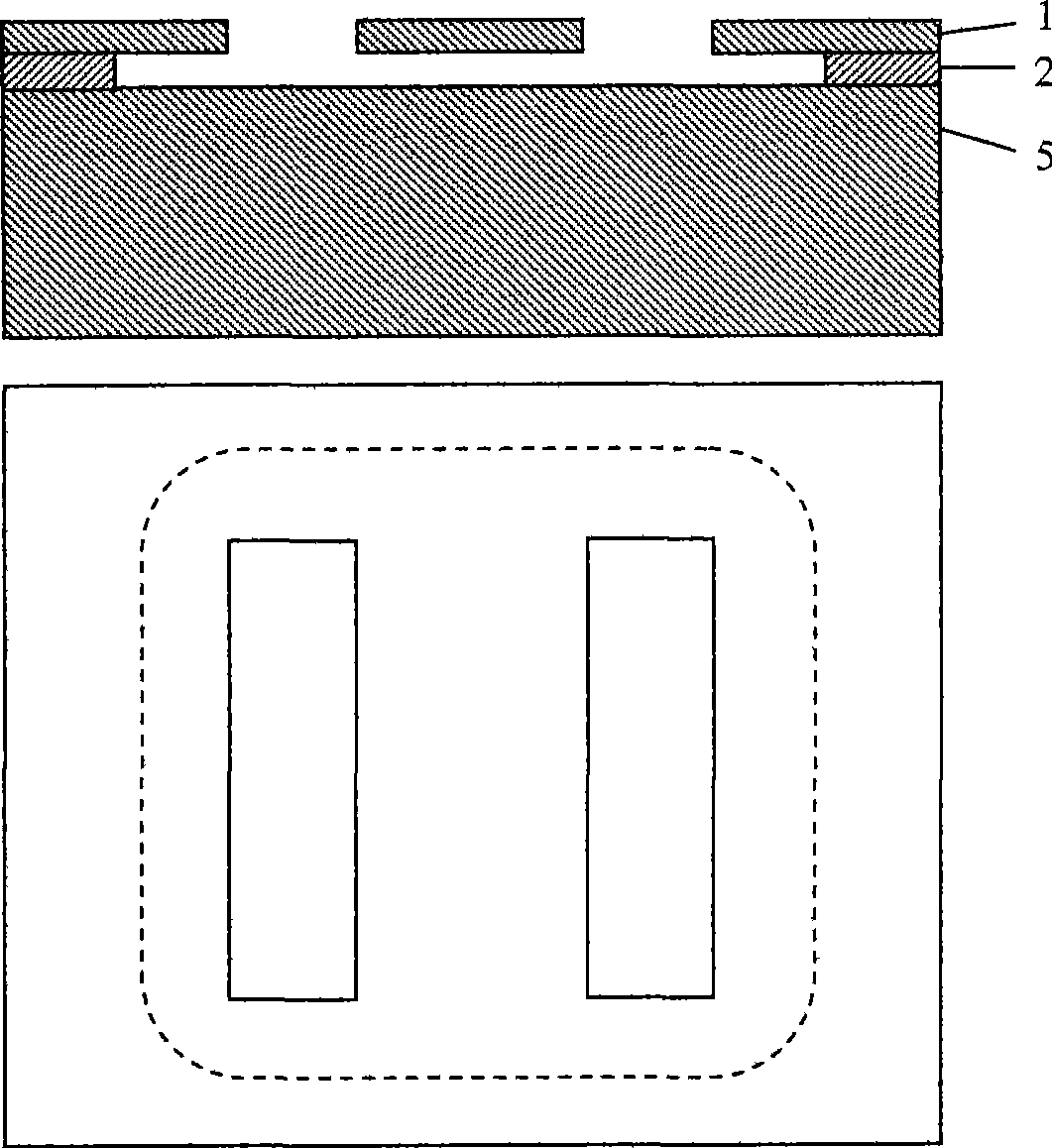
[0023] (3), SOI intermediate insulating layer S...


PUM

PropertyMeasurementUnit
Lengthaaaaaaaaaa
Thicknessaaaaaaaaaa
Thicknessaaaaaaaaaa

Abstract

The invention relates to the technical field of micro-electronics technique and a device thereof, in particular to a preparation method of a novel piezoelectric membrane resonator. The invention is characterized in that an SOI wafer is adopted to etch a plurality of etch baths or etch pits on a top layer of silicon; then hydrofluoric acid is used for etching an insulating layer in the surrounded range among the baths or pits; a suspended silicon layer is formed on the top layer of the wafer; next, a bottom electrode material, a piezoelectric membrane material and a top electrode material are deposited on the suspended top layer of silicon in sequence so as to form the piezoelectric membrane resonator. The invention has the beneficial effects that the SOI wafer is adopted to manufacture a cavity-typed piezoelectric membrane resonator; wherein, an oxide layer between two layers of silicon is used as a sacrificial layer, thus saving the step of depositing the sacrificial layer and simplifying the technique; besides, the sacrificial layer is compatible with the silicon technique, therefore, a resonator array and an external circuit are integrated so as to lead the circuit to has the advantages of high speed, low voltage, low power consumption, high sensitivity, fast response speed and multiple channels and simultaneously lead the device to have higher degree of micromation and integration.

Description

[technical field] [0001] The invention relates to the technical field of microelectronic technology and devices thereof, in particular to a preparation method of a novel piezoelectric thin film resonator. [Background technique] [0002] For traditional quartz resonators, the operating frequency of the fundamental mode is limited by the thickness of the crystal. Even if the ion beam processing method is used to reduce the thickness to 30um, it is difficult to obtain a frequency exceeding 200MHz. At present, the crystal that works according to the fundamental frequency can only reach about 25MHz. Moreover, conventional piezoelectric resonator processes are not compatible with silicon processes for integrated circuits. [0003] For bulk acoustic wave (bulk acoustic wave) piezoelectric thin film resonators fabricated on silicon wafers, although its working principle is the same as that of low-frequency quartz crystal resonators, since the thickness of piezoelectric thin film re...

Claims


Application Information

Patent Timeline
IPC IPC(8): H03H3/02H01L41/22
Inventor 言智邓沛然刘延辉周细应于治水
Owner SHANGHAI UNIV OF ENG SCI
Why Eureka
Try Eureka