On-site programmable device FPGA logic unit model and general bin packing algorithm thereof

A technology of logic unit and box packing algorithm, which is applied in the direction of instruments, calculations, and special data processing applications, etc., and can solve problems such as too simple connections, too simple functions, and inapplicability

Inactive Publication Date: 2009-08-26
FUDAN UNIV
View PDF0 Cites 24 Cited by
  • Summary
  • Abstract
  • Description
  • Claims
  • Application Information

AI Technical Summary

Problems solved by technology

[0004] A logic cluster is the simplest structural model of a hierarchical logic block. Its internal logic unit BLE and internal interconnection switch matrix adopt the most simplified method. Its shortcomings are: first, the logic unit BLE structure It is the simplest structure that can realize combinational or sequential logic, does not contain any special devices, and the described function is too simple, which is not applicable in the actual application field of commercial FPGA; second, the internal interconnection switch matrix is ​​fully connected, Causes a

Method used


Image

  • On-site programmable device FPGA logic unit model and general bin packing algorithm thereof
  • On-site programmable device FPGA logic unit model and general bin packing algorithm thereof
  • On-site programmable device FPGA logic unit model and general bin packing algorithm thereof

Examples


Embodiment Construction

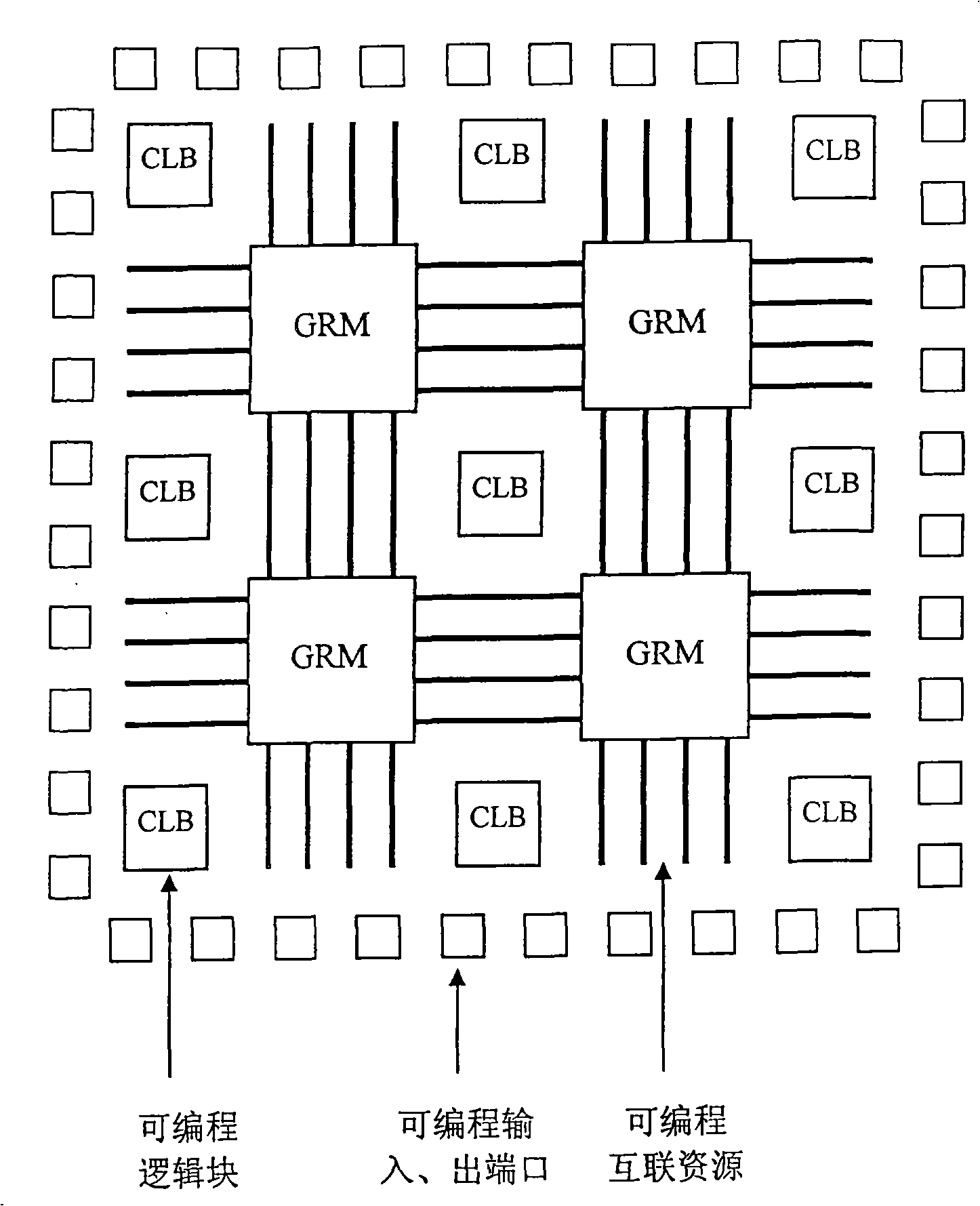
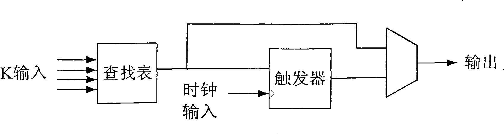
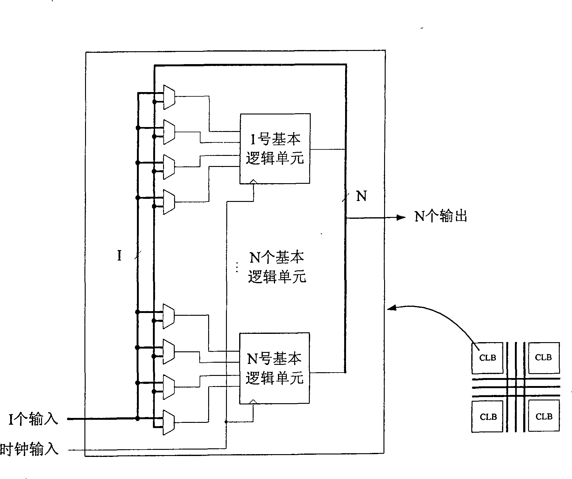
[0126] attached Figure 4 , attached Figure 5 And attached Image 6 It is the logic unit structure diagram of three series FPGAs of Xilinx Company. According to the functions of user circuits that FPGA can realize, the circuits can be divided into three categories: 1) Logic functions composed of special devices; 2) Logic functions composed of look-up tables and flip-flops Logical functions composed of special devices; 3) Logical functions composed of IP cores such as CPU, RAM blocks, and DSP cores. Among them, the user circuits completed by the logic unit are only 1) and 2). The present invention simplifies the logical units realizing the user circuit 1) and 2) into a three-level model according to the mutual driving conditions of various devices: the first level is a lookup table, the second level is a special device, and the third level is a sequential device ,Such as Figure 7shown. The lookup table is used to map the combinational logic of any K input, and at the sam...


PUM


Abstract

The invention relates to an on-site programmable device FPGA logic unit model and a general bin packing algorithm thereof. The module is analyzed and modeled according to realizable subscriber circuit logic function type in logic unit, and can be divided into three stages according to mutual driving case, the first stage is a searching table, the second stage is a special device, and the third stage is a sequential device, and the model can widely describe present commercial FPGA chip logic unit structure. Based on the module, the invention provides a general logic unit bin packing algorithm from bottom to top, which respectively establish user-defined logic devices for a device using the special device as core, a device using the sequential device as core and a device using the searching table as core in subscriber circuit, and carries out bin packing for the self- established devices by employing gain function calculation. The algorithm is a universal algorithm for treating bin packing problem of various logic units, has wide representation, versatility, practicality and excellent time spending performance, and is suitable for large-scale subscriber circuit.

Description

technical field [0001] The invention belongs to the electronic design automation (Electronic Design Automation, EDA) technical field of Field Programmable Gate Array (FPGA), be specifically related to a kind of model of FPGA logic unit and a kind of logic unit of Field Programmable Gate Array based on lookup table Generic bin packing algorithm. technical background [0002] Literature [1] points out that a logic block (Configurable Logic Block) is a component used to implement user circuit logic in a field programmable gate array (Field Programmable Logic Array, FPGA). Block (Configurable I / O Block) is the three important components of FPGA, such as figure 1 shown. [0003] With the development of the FPGA structure, the logic block gradually develops into a hierarchical logic block and becomes the mainstream. Hierarchical logic block (also known as cluster structure logic block, which contains multiple logic units) puts the line network that originally needs to use inter...

Claims


Application Information

Patent Timeline
IPC IPC(8): G06F17/50
Inventor 杨萌王侃文周学功童家榕
Owner FUDAN UNIV
Why Eureka
Try Eureka