Double-faced exposure architecture and double-faced exposure method of printed circuit board

A printed circuit board, double-sided exposure technology, applied in the direction of printed circuit, printed circuit manufacturing, microlithography exposure equipment, etc., can solve the problems of inconvenience, general products and methods without suitable structures and methods, and avoid scratches Effect

Inactive Publication Date: 2009-09-02
CHIME BALL TECH
View PDF0 Cites 12 Cited by
  • Summary
  • Abstract
  • Description
  • Claims
  • Application Information

AI Technical Summary

Problems solved by technology

[0005] It can be seen that the above-mentioned existing printed circuit board double-side exposure framework and double-side exposure method obviously still have inconveniences and defects in product structure, method and use, and need to be further improved urgently.
In order to solve the above-mentioned problems, the

Method used


Image

  • Double-faced exposure architecture and double-faced exposure method of printed circuit board
  • Double-faced exposure architecture and double-faced exposure method of printed circuit board
  • Double-faced exposure architecture and double-faced exposure method of printed circuit board

Examples


Embodiment Construction

[0057] In order to further explain the technical means and effects of the present invention to achieve the intended purpose of the invention, the following is a specific implementation of the double-sided exposure structure and double-sided exposure method for printed circuit boards proposed in accordance with the present invention in conjunction with the accompanying drawings and preferred embodiments. The manner, structure, method, steps, features and effects thereof are described in detail below.

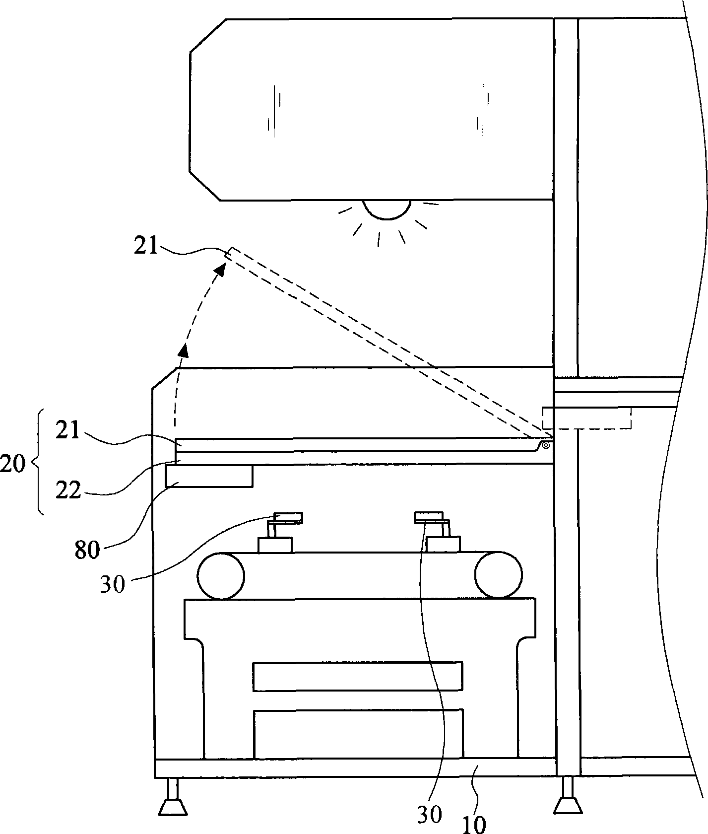
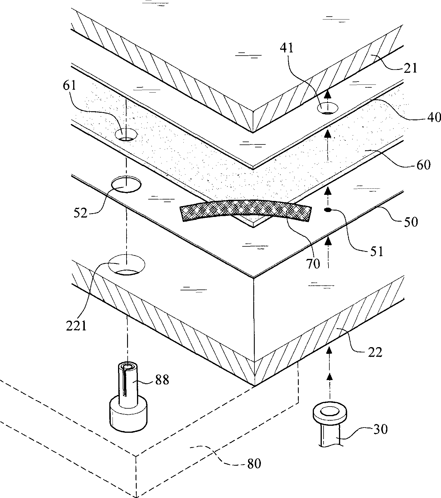
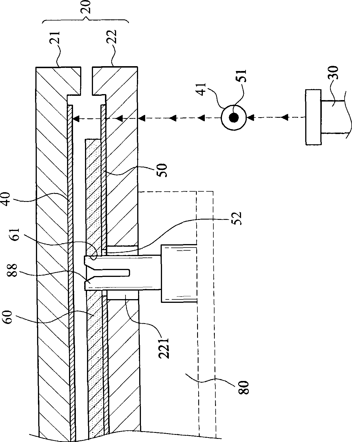
[0058] With reference figure 1 , a schematic diagram of the double-sided exposure architecture of the printed circuit board of the present invention. As shown in the figure, a double-sided exposure device 10 applying the double-sided exposure framework of the present invention includes an exposure frame 20, an exposure upper frame 21 and an exposure lower frame 22, and the exposure upper frame 21 can be covered with The lower frame 22 is exposed, and the alignment device 80 is d...


PUM


Abstract

The invention relates to a double-faced exposure architecture and a double-faced exposure method of a printed circuit board. The double-faced exposure architecture at least comprises an exposure frame, an aligning lens, an upper photographic plate, a lower photographic plate, a rigid clapboard and an aligning device, and the upper photographic plate and the lower photographic plate are separated by the rigid clapboard, thus avoiding scratching, and the lower photographic plate is aligned with a previously arranged exposure location of the upper photographic plate through the aligning lens, thus achieving the goal of double-faced exposure aligning of the printed circuit board.

Description

technical field [0001] The invention relates to a double-side exposure structure and a double-side exposure method, in particular to a double-side exposure structure and a double-side exposure method for double-side exposure alignment of a printed circuit board. Background technique [0002] The double-sided exposure technology of the printed circuit board is to place the printed circuit board in the exposure frame of the double-sided exposure machine, and through the positioning of the upper film and the lower film, and then sandwich the printed circuit board to be exposed between the upper film and the lower film. Between the lower negatives, according to the alignment image captured by the CCD camera, the printed circuit board needs to be aligned with the upper and lower negatives relative to the exposure position, and then double-sided exposure is performed. However, before the upper film and the lower film are positioned on the upper frame and the lower frame of the exp...

Claims


Application Information

Patent Timeline
IPC IPC(8): G03F7/20H05K3/00
Inventor 张鸿明
Owner CHIME BALL TECH
Why Eureka
Try Eureka