

Iii-nitride light-emitting devices with one or more resonance reflectors and reflective engineered growth templates for such devices, and methods
A technology of nitride and nitride layer, which is applied in the direction of lasers, semiconductor devices, electric solid-state devices, etc., can solve the problem of difficult commercialization and high yield of etching process
- Summary
- Abstract
- Description
- Claims
- Application Information
AI Technical Summary
Problems solved by technology
Method used
Image

Examples
no. 1 approach
[0093] exist Image 6 with Figure 7 The structure and energy band diagram of the first embodiment are shown in , respectively.
[0094] GEMM(604) is suitable for various forms of optical cavity semiconductor light emitters. In a first embodiment, the GEMM (604) with its highly reflective bulk properties can be grown thinner such that the GEMM (604) is partially transparent and partially reflective. The first embodiment utilizes a device-quality planar III-nitride material growth template consisting of a sapphire substrate (601), an i-GaN buffer layer (602), and an n-GaN layer (603), such that the GEMM (604) The crystal quality is planar, specular and device quality. The GEMM (604) is lattice matched to the n-GaN layer (603) so that the required thickness can be below the epitaxial critical thickness.
[0095] Once a 2μm i-GaN buffer layer (602) and a 2μm n-GaN layer (603) are grown on the sapphire substrate (601), the GEMM (604) can be grown to a specific thickness for th...
Embodiment approach
[0098] For this implementation, the following factors should be considered:
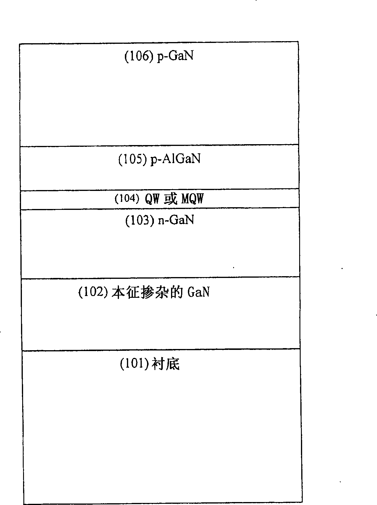
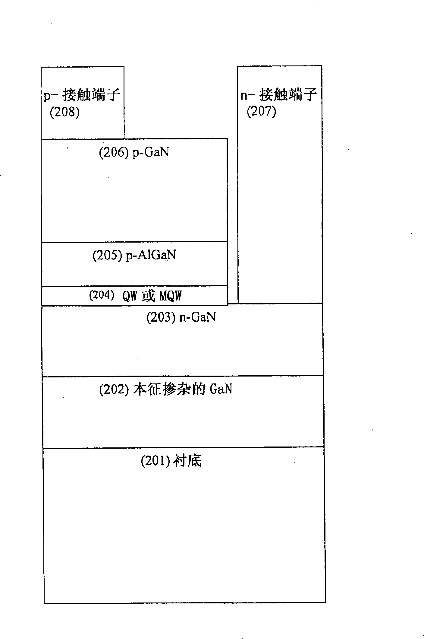
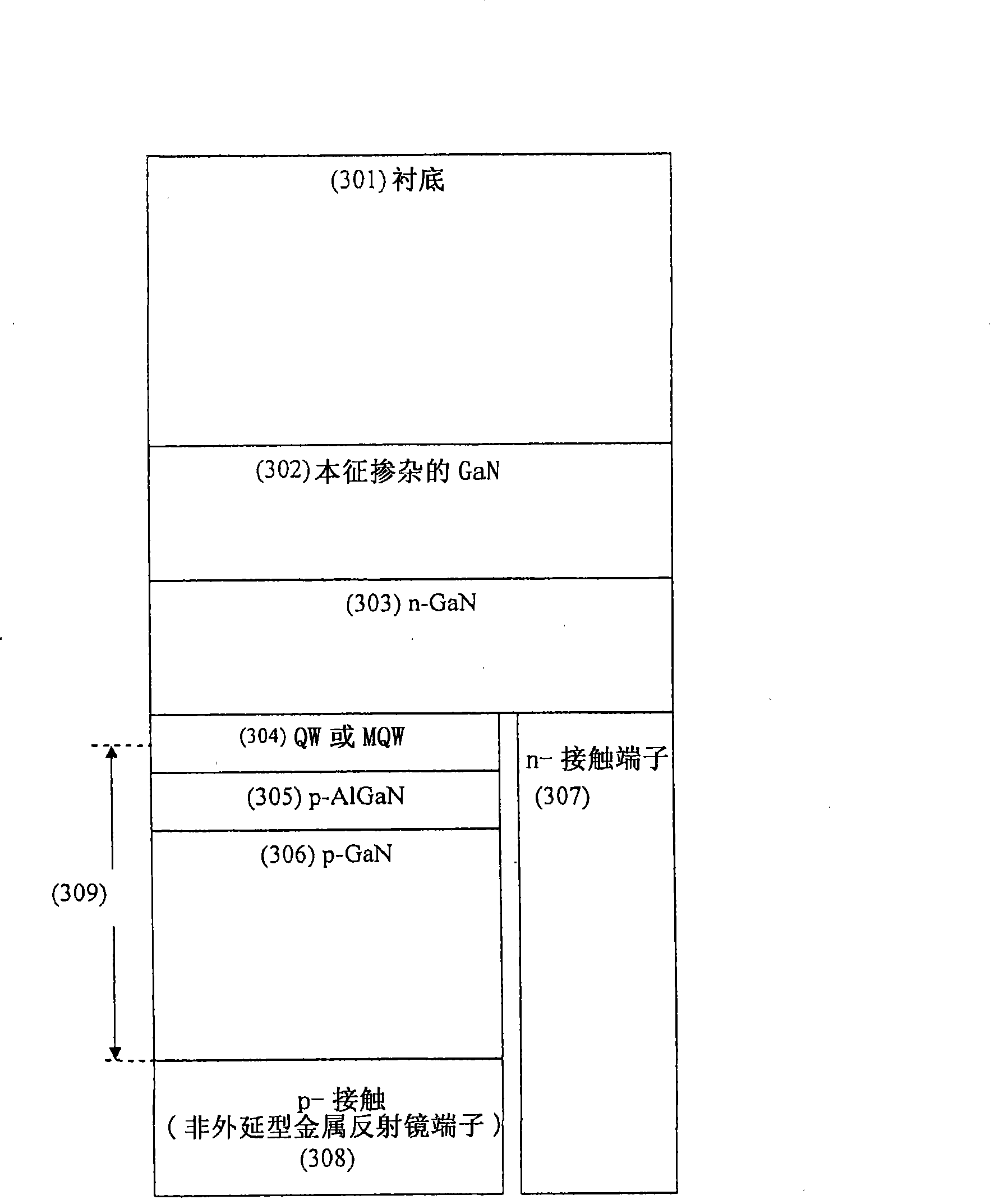
[0099] a. A planar n-type GaN layer template (603) with device quality;
[0100] b. the thickness, flatness, specular reflectivity and transparency of the GEMM layer (604) grown on the first n-type GaN layer (603);
[0101] c. The thickness of the second n-type conducting layer (605) grown on the GEMM (604) and having device quality;
[0102] d. The position of the active region (606) relative to the enclosing mirrors (604), (610);
[0103] e. the thickness of the p-type conductive layer (607) (608); and
[0104]f. Reflective properties of non-epitaxial metal contacts (610).
[0105] Although the device efficiency is superior to that of standard LEDs, it may be of interest to detune the device in its configuration such that improvements in directivity and spectral narrowing replace even higher light extraction efficiency. This can be done by keeping all parameters the same while increasing the w...
no. 2 approach
[0112] exist Figure 8 with 9 The structure and energy band diagram of the second embodiment are shown in , respectively.
[0113] GEMM(804) is suitable for various forms of optical cavity semiconductor light emitters. In a second embodiment, the GEMM (804) with its highly reflective bulk properties can be grown thick such that the GEMM (804) exhibits its bulk reflectivity. The second embodiment utilizes a device-quality planar III-nitride material growth template consisting of a sapphire substrate (801), an i-GaN buffer layer (802) and an n-GaN layer (803), such that the GEMM (804) The crystal properties of the crystals are planar, specular, and device-quality. The GEMM (804) is lattice matched to the n-GaN layer (803), so that the required thickness can be below the epitaxial critical thickness.
[0114] Once a 2 μm i-GaN buffer layer (802) and a 2 μm n-GaN layer (803) are grown on the sapphire substrate (801), the GEMM (804) can be grown to a thickness for the resonant ...
PUM
 Abstract
Description
Claims
Application Information