Eureka AIR delivers breakthrough ideas for toughest innovation challenges, trusted by R&D personnel around the world.

Substrate surface temperature measurement method, substrate processing apparatus using the same, and semiconductor device manufacturing method

A temperature measurement and substrate surface technology, which is applied in semiconductor/solid-state device manufacturing, semiconductor/solid-state device testing/measurement, thermometers, etc., can solve problems such as error, difficulty in keeping the sensor in contact with the substrate, substrate waste, etc., to improve measurement The effect of precision

Inactive Publication Date: 2009-09-09
CANON ANELVA CORP
View PDF3 Cites 13 Cited by
  • Summary
  • Abstract
  • Description
  • Claims
  • Application Information

AI Technical Summary

Problems solved by technology

When the sensor is brought into contact with the substrate surface in this way, or when the substrate expands due to temperature changes in the substrate, it is difficult to maintain the sensor in contact with the substrate
Also, errors can occur when the thermocouple itself is heated by the heater
Since no film is formed on the part of the substrate that is in contact with the sensor, the substrate is partially wasted

Method used


Image

  • Substrate surface temperature measurement method, substrate processing apparatus using the same, and semiconductor device manufacturing method
  • Substrate surface temperature measurement method, substrate processing apparatus using the same, and semiconductor device manufacturing method
  • Substrate surface temperature measurement method, substrate processing apparatus using the same, and semiconductor device manufacturing method

Examples


no. 1 example

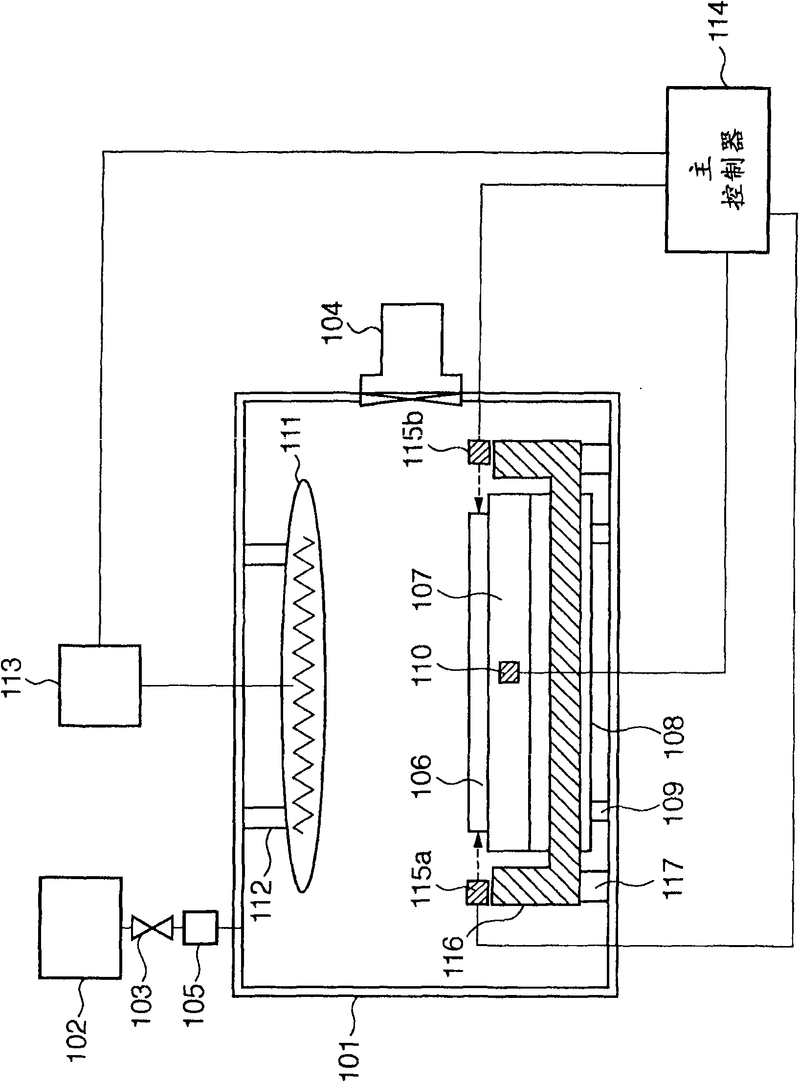
[0068] figure 1 The arrangement of a thermal CVD apparatus according to a first embodiment of the invention is schematically shown.

[0069] A substrate processing apparatus used as the thermal CVD apparatus of this embodiment includes a vacuum vessel 101 , and a film is formed on a substrate 106 in the vacuum vessel 101 . A source gas supply device 102 and a vacuum pump 104 are supplied to the vacuum container 101 . The source gas supply device 102 supplies a film source gas to the vacuum vessel 101 . The supply path of the source gas has a valve 103 and a flow controller 105 that adjusts the concentration of the source gas.

[0070] The vacuum vessel 101 has an electrostatic chuck 107 and a substrate stage 108 at its inner bottom. The electrostatic chuck 107 fixes the substrate 106 at a predetermined position. The substrate stage 108 suppresses deformation of the electrostatic chuck 107 . The substrate stage 108 is connected to the vacuum vessel 101 by an attachment me...

no. 2 example

[0112] Figure 5 The arrangement of a thermal CVD apparatus according to a second embodiment of the invention is schematically shown.

[0113] The device of this embodiment is achieved by figure 1 The arrangement obtained by adding the observer stage temperature sensor 118. The scope stage temperature sensor 118 serves as support body temperature detection means for detecting the temperature of the scope stage 116 . In addition, an observer stage temperature control tube 119 and an observer stage temperature controller 120 are added. The observer stand temperature control pipe 119 is laid in the observer stand 116 to adjust the temperature of the observer stand 116 . The observer stage temperature controller 120 controls the circulation of the refrigerant flowing in the tube 119 .

[0114] When the refrigerant circulates in the observer stage temperature control pipe 119, the reduction of temperature non-uniformity in the observer stage 116 can be more than that in the ob...

no. 3 example

[0129] Figure 6 The arrangement of a thermal CVD apparatus according to a third embodiment of the present invention is schematically shown. In the description of this example, with figure 1 and 5 The same constituent components of the devices shown in are denoted by the same reference numerals, and repeated descriptions will be omitted.

[0130] In a third embodiment, no halogen heater is provided above the substrate surface (see figure 1 and 2 Reference number 111 in . like Figure 6 As shown, a heater 121 disposed in the substrate stage 108 heats the substrate 106 . The heater 121 is connected to a heater controller 122 . The heater controller 122 is connected to the main controller 114 .

[0131] The upper surface of the substrate 106 has alignment marks 126 at multiple portions. The positions of the alignment marks 126 can be detected by the alignment scopes 123a and 123b located above them. Alignment scopes 123 a and 123 b are attached to scope rig 124 . The...


PUM

PropertyMeasurementUnit
thicknessaaaaaaaaaa
thermal conductivityaaaaaaaaaa

Abstract

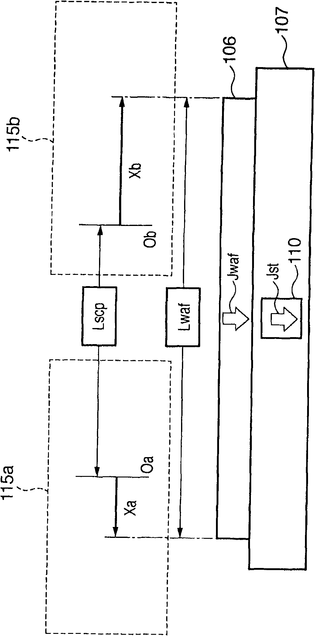
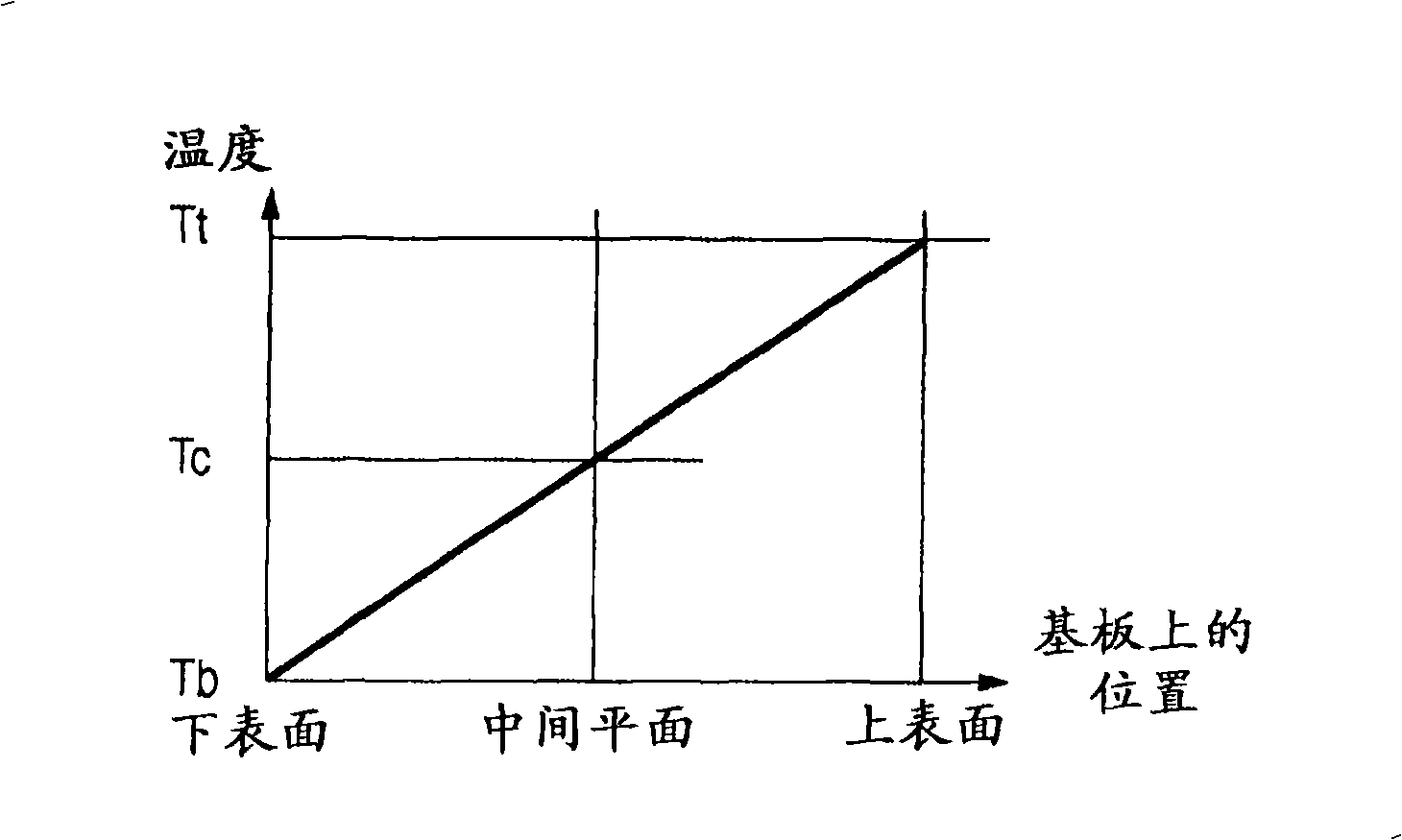
The present invention relates to a substrate surface temperature measurement method, a substrate processing apparatus using the same and a semiconductor device manufacturing method. The expansion amount of a substrate (106) is measured using a scope (115a, 115b) which observes the edge surface of the substrate (106). The temperature of the neutral plane of the substrate (106) is calculated using the expansion amount of the substrate (106). A heat flux in the substrate (106) is measured using a heat flux sensor (110). The temperature difference between the neutral surface and upper surface of the substrate (106) is calculated from the measured heat flux and the heat resistance of the substrate (106). The temperature of the surface of the substrate (106) is obtained using the temperature difference and the temperature of the neutral plane of the substrate.

Description

technical field [0001] The present invention relates to a substrate surface temperature measuring method for measuring the substrate surface temperature in situ in an apparatus for heating and cooling a substrate in the process of manufacturing electronic devices such as semiconductor integrated circuits and electron sources for display devices, and a substrate processing using the method Apparatus, and a method for manufacturing a semiconductor device. Background technique [0002] Semiconductor integrated circuit manufacturing processes include various types of annealing processes such as baking, film formation, and ashing in photolithography. In such an annealing process, the target substrate is conventionally heated using a halogen lamp arranged opposite to the target substrate or a heater incorporated into a support supporting the target substrate. [0003] In this case, the radiation thermometer is arranged across the target substrate on the side opposite to the halog...

Claims


Application Information

Patent Timeline
Patent Type & Authority Applications(China)
IPC IPC(8): H01L21/66G01K7/02H01L21/00H01L21/02H01L21/324
CPCG01K5/486H01L22/12G01K7/42G01K5/50
Inventor 山本武
Owner CANON ANELVA CORP
Why Eureka
Eureka Blog
Learn More