Carrier leak correcting circuit used at front end of emission and method thereof

A technology of carrier leakage and correction circuit, applied in transmitter monitoring, electrical components, transmission monitoring, etc., can solve the problems of carrier leakage, correction circuit power consumption and large chip area, and achieve low power consumption and small chip area. Effect

Inactive Publication Date: 2009-09-23
BEIJING RFMC TECH CORP
View PDF2 Cites 13 Cited by
  • Summary
  • Abstract
  • Description
  • Claims
  • Application Information

AI Technical Summary

Problems solved by technology

[0007] The purpose of the present invention is to provide a carrier leakage correction circuit and correction method for the transmitting front-end, which can solve the problem that the correction circuit of the transmitting front-end carrier leakage in the prior art needs to use a radio frequency detector, resulting in large power consumption and chip area of ​​the correction circuit The problem

Method used


Image

  • Carrier leak correcting circuit used at front end of emission and method thereof
  • Carrier leak correcting circuit used at front end of emission and method thereof
  • Carrier leak correcting circuit used at front end of emission and method thereof

Examples


Embodiment Construction

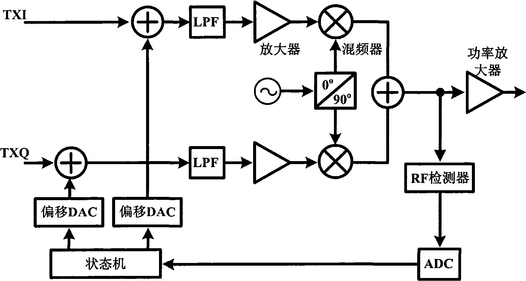
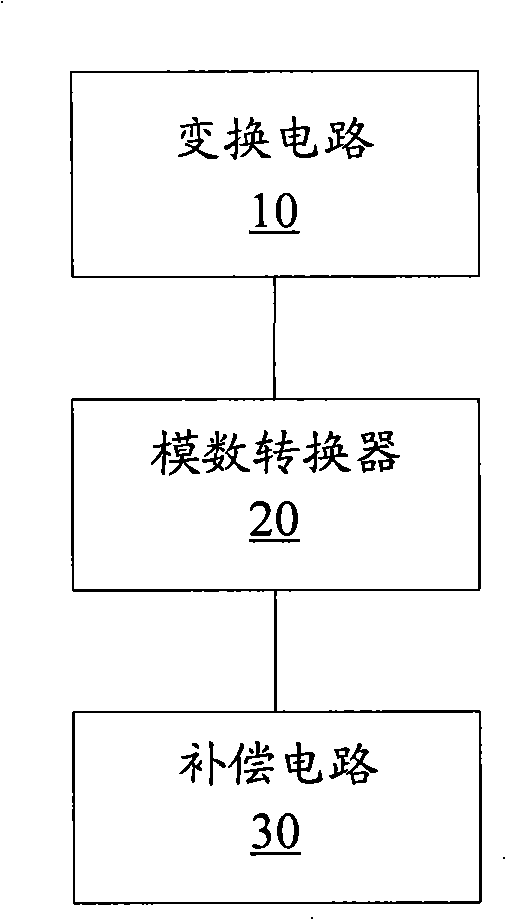
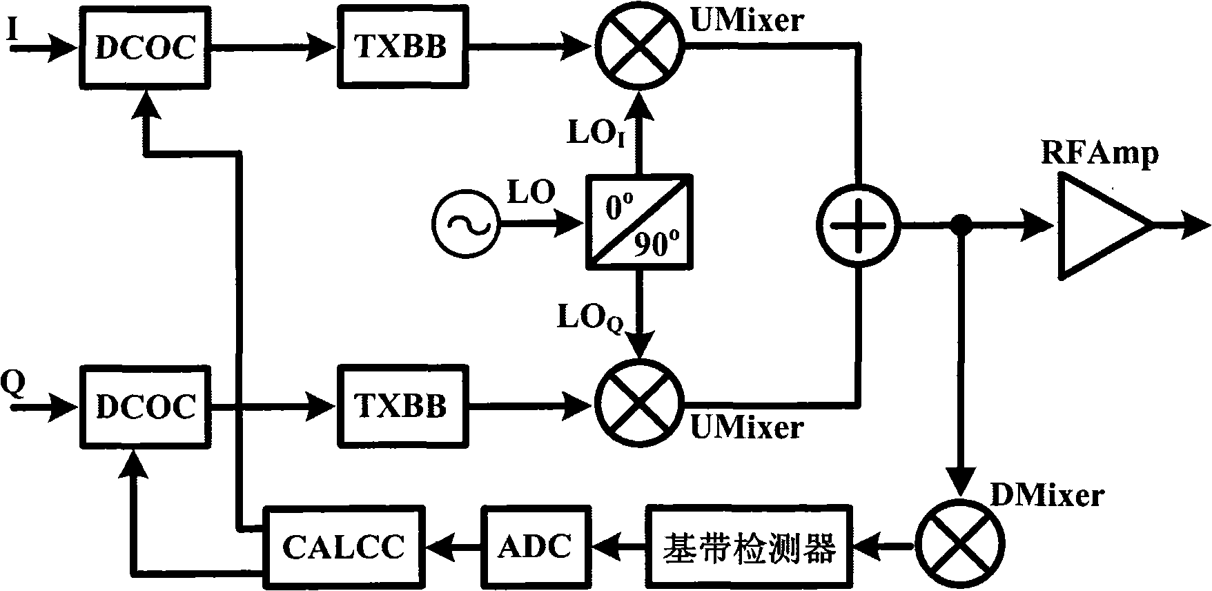
[0027] The present invention will be described in detail below with reference to the accompanying drawings and in combination with embodiments.

[0028] figure 2 A structural diagram of a carrier leakage correction circuit for a transmitting front end according to an embodiment of the present invention is shown, including:

[0029] Transformation circuit 10, for transforming the carrier leakage signal into an analog baseband signal;

[0030] Analog-to-digital converter 20, for converting the analog baseband signal into a digital signal;

[0031] The compensation circuit 30 is configured to compensate the analog baseband processing circuit of the transmitting front end according to the digital signal.

[0032] In the above embodiment, the carrier leakage signal is converted into an analog baseband signal by the conversion circuit 10, the analog baseband signal is converted into a digital signal by the analog-to-digital converter 20, and the analog baseband processing circuit...


PUM


Abstract

The invention provides a carrier leak correcting circuit used at the front end of emission, comprising a converting circuit used for converting a carrier leak signal into an analog baseband signal, an analog-to-digital converter used for converting the analog baseband signal into a digital signal, and a compensating circuit used for compensating an analog baseband processing circuit at the front end of emission according to the digital signal. The invention also provides a carrier leak correcting method used at the front end of emission, comprising the following steps: down-frequency conversion is realized on the carrier leak signal, so that the analog baseband signal of carrier leakage can be obtained; a baseband signal intensity detector can be used for detecting the analog baseband signal of carrier leakage, and analog-to-digital conversion is realized on the detected signal, so that the digital signal of carrier leakage can be obtained; according to the digital signal of carrier leakage, DC Offset compensation realized in the analog baseband processing circuit at the front end of emission by the compensating circuit. The invention realizes the technical effects of lower power consumption of the correcting circuit and smaller area of a chip.

Description

technical field [0001] The present invention relates to the field of integrated circuits, in particular to a carrier leakage correction circuit and method for a transmitting front end. Background technique [0002] The transmission front-end with zero-IF or low-IF structure does not require an off-chip image rejection filter, has small power consumption and area, and is highly integrated, so it is widely used. However, due to capacitance, substrate coupling, or baseband DC offset, the carrier ( That is, the local oscillator) signal enters the output spectrum of the radio frequency transmitting front end, that is, a carrier leak (Carrier Leak, CL for short) is generated. Carrier leakage has the following adverse effects: deterioration of the linearity of the post-stage circuit (power amplifier, etc.), resulting in the offset of the origin of the transmitted signal constellation diagram; after being transmitted with the carrier, it will cause interference to other RF front end...

Claims


Application Information

Patent Timeline
Patent Type & Authority Applications(China)
IPC IPC(8): H04B17/00H04B1/04H04B17/11
Inventor 刘瑞峰李卓王玉花陈永聪王文申
Owner BEIJING RFMC TECH CORP
Why Eureka
Try Eureka