Semiconductor device and manufacturing method of same

A technology of semiconductors and devices, applied in the field of semiconductor devices and their manufacturing, capable of solving problems such as SMT without giving any clear guidance, without establishing FinFET or nanowire transistors

Active Publication Date: 2009-09-30
TOSHIBA MEMORY CORP
View PDF1 Cites 26 Cited by
  • Summary
  • Abstract
  • Description
  • Claims
  • Application Information

AI Technical Summary

Problems solved by technology

However, no clear guidance has been given for applying strain to the channel region of FinFET or nanowire transistors to imp...

Method used


Image

  • Semiconductor device and manufacturing method of same
  • Semiconductor device and manufacturing method of same
  • Semiconductor device and manufacturing method of same

Examples


no. 1 example

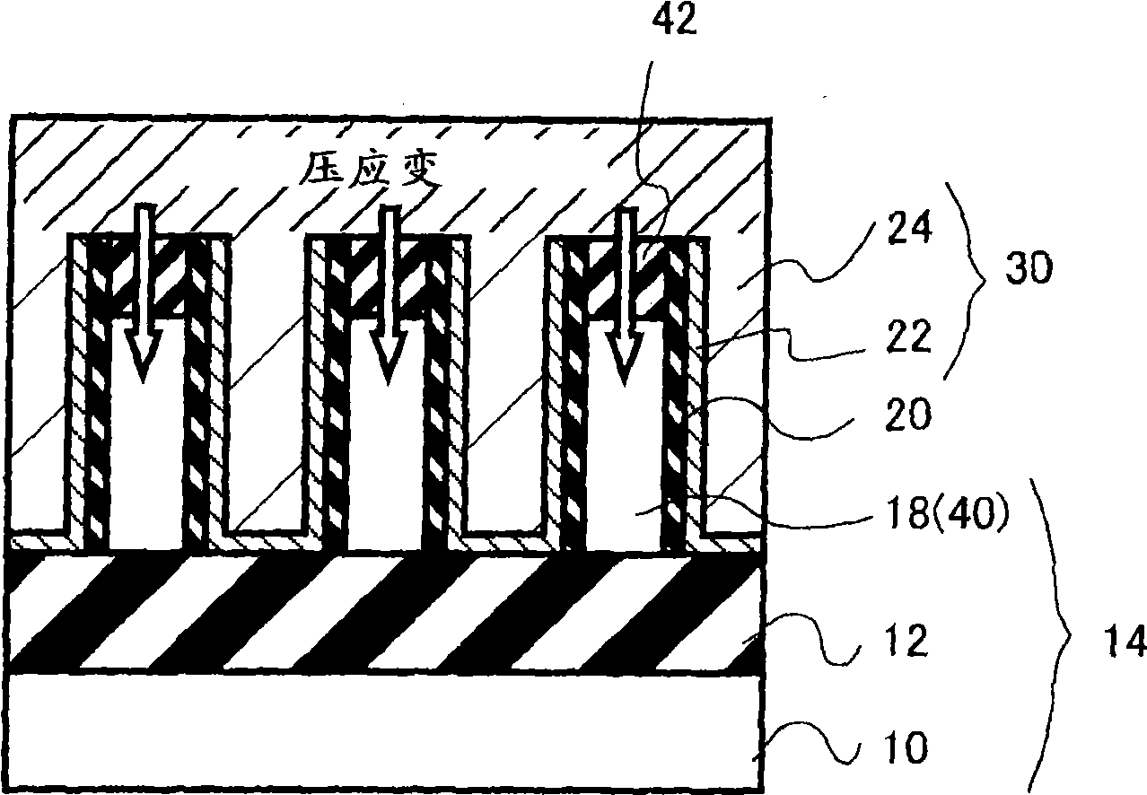
[0048] The semiconductor device according to the present embodiment is configured to include: a semiconductor substrate; a cuboid-shaped semiconductor layer formed on the upper portion of the semiconductor substrate and having a top surface parallel to the main surface of the semiconductor substrate and a surface perpendicular to the semiconductor substrate. (100) plane oriented sides of the main surface of the bottom; and a p-channel Metal Insulator Semiconductor Field Effect Transistor (pMISFET). The pMISFET has: a channel region formed at least at the side surfaces of the cuboid-shaped semiconductor layer; a gate dielectric film formed at least at the side surfaces of the cuboid-shaped semiconductor layer; a gate electrode covering the channel region, the gate a dielectric film sandwiched between the gate electrode and the channel region; and a pair of source / drain regions formed in the rectangular parallelepiped-shaped semiconductor layer in such a manner that the channel r...

no. 2 example

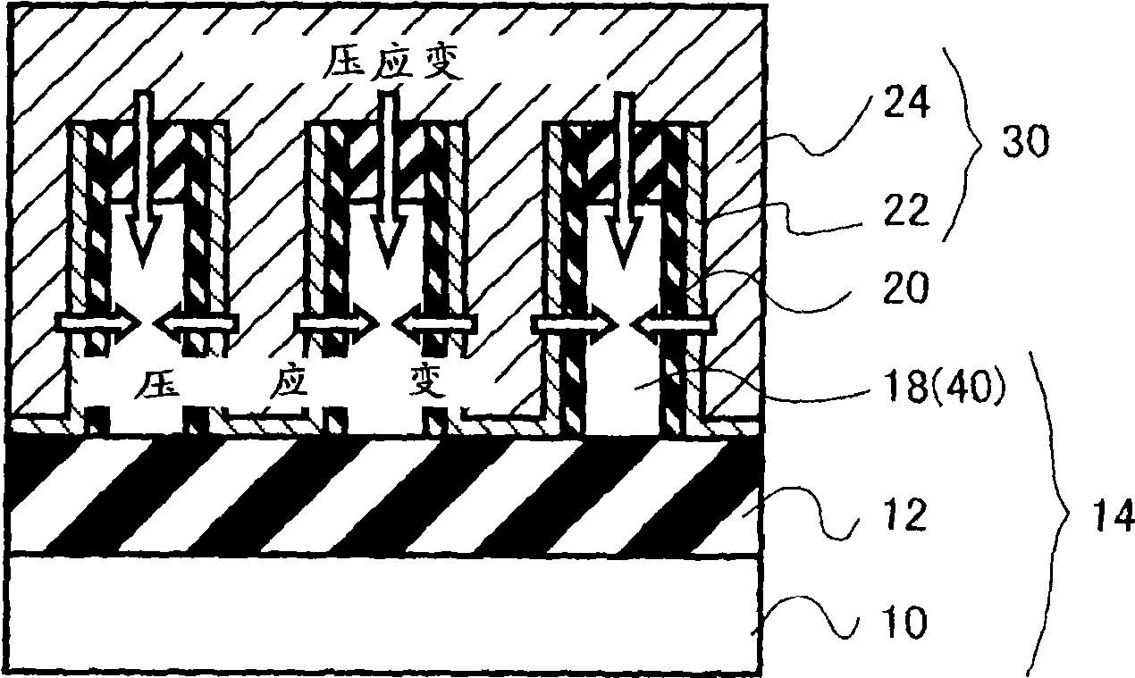
[0072] The semiconductor device of the present embodiment is a p-channel nanowire transistor, which is compatible with figure 1 Similar to the semiconductor device of the first embodiment shown in , in which the hard mask layer 42 is removed and is also formed on the top surface of the rectangular semiconductor layer 40, that is, on the upper surface of the channel region 18 by interposing the gate insulating film A gate electrode is provided. The present embodiment is similar to the first embodiment except that the structure of a FinFET is used as the nanowire transistor structure; therefore, descriptions thereof will be omitted.

[0073] Figure 15 is a schematic cross-sectional view of the semiconductor device of this embodiment in a direction at right angles to its gate length direction. Such as Figure 15 As shown in , the gate insulating film 20 is also formed on the upper surface of the channel region 18 formed at the cuboid-shaped semiconductor layer 40 having the (...

no. 3 example

[0086] The semiconductor device of this embodiment is a p-channel FinFET, and figure 1 Similar to the semiconductor device of the first embodiment shown in , in which the semiconductor film of the gate electrode is modified such that its lowermost surface is above the top surface of the cuboid-shaped semiconductor layer. Except for this structural difference, the device is the same as the first embodiment; therefore, repeated description will be omitted here.

[0087] Figure 22 is a schematic cross-sectional view of the semiconductor device of this embodiment in a direction at right angles to its gate length direction. like Figure 22 As shown in , the lowermost surface of the polysilicon film 24 of the gate electrode 30 is provided to cover the upper surface of the channel region 18 , that is, the top surface of the rectangular semiconductor layer 40 . In other words, it becomes a structure in which the space between adjacent channel regions 18 (rectangular semiconductor ...


PUM

PropertyMeasurementUnit
Heightaaaaaaaaaa

Abstract

A FinFET and nanowire transistor with strain direction optimized in accordance with the sideface orientation and carrier polarity and an SMT-introduced manufacturing method for achieving the same are provided. A semiconductor device includes a pMISFET having a semiconductor substrate; a rectangular solid-shaped semiconductor layer formed at upper part of the substrate to have a top surface parallel to a principal plane of the substrate and a sideface with a (100) plane perpendicular to the substrate's principal plane; a channel region formed in the rectangular semiconductor layer; a gate insulating film formed at least on the sideface of the rectangular layer; a gate electrode on the gate insulator film; and source/drain regions formed in the rectangular semiconductor layer to interpose the channel region therebetween. The channel region is applied a compressive strain in the perpendicular direction to the substrate principal plane. A manufacturing method of the device is also disclosed.

Description

[0001] Cross References to Related Applications [0002] This application is based on and claims the benefit of priority from Japanese Patent Application No. 2008-085905 filed on March 28, 2008, the entire contents of which are hereby incorporated by reference. technical field [0003] Exemplary embodiments described herein relate to semiconductor devices having "fin" type (fin) type (fin) channel transistors or nano-wire (nano-wire) channel transistors and methods of manufacturing the same. Background technique [0004] Fin-channel MISFET (FinFET) structures with enhanced resistance to short-channel effects and nanowire-channel transistors (nanowire transistors) are expected to be used as the basis for realizing ultra-thin devices with gate lengths of 30 nanometers (nm) or less. Device structure of a miniaturized metal-insulator-semiconductor field-effect transistor (MISFET). For example, a FinFET is designed to have a rectangular parallelepiped-shaped semiconductor layer ...

Claims


Application Information

Patent Timeline
IPC IPC(8): H01L27/088H01L29/10H01L21/8234
CPCH01L29/7843H01L29/7842H01L29/785H01L29/66795H01L21/823807H01L29/0676H01L29/0673H01L21/823821
Inventor 斋藤真澄内田建
Owner TOSHIBA MEMORY CORP
Why Eureka
Try Eureka