

Microelectronic assembly and method for forming the same
A technology of microelectronics and components, applied in the direction of electrical components, electric solid devices, circuits, etc., can solve the problems of increasing the manufacturing cost of the device, increasing the thickness of the coil, increasing the size, etc.
- Summary
- Abstract
- Description
- Claims
- Application Information
AI Technical Summary
Problems solved by technology
Method used
Image

Examples
Embodiment Construction
[0024] The following detailed description is exemplary only in nature and is not intended to limit the invention or the application and uses of the invention. Furthermore, there is no intention to be bound by any theory expressed or implied in the preceding technical field, background, brief summary or the following detailed description. Note also that Figure 1-18 They are merely illustrative and may not be drawn to scale.
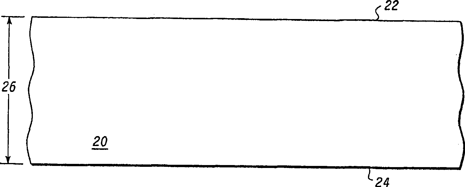
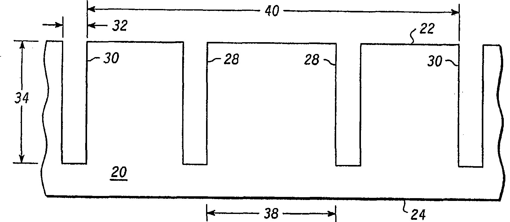
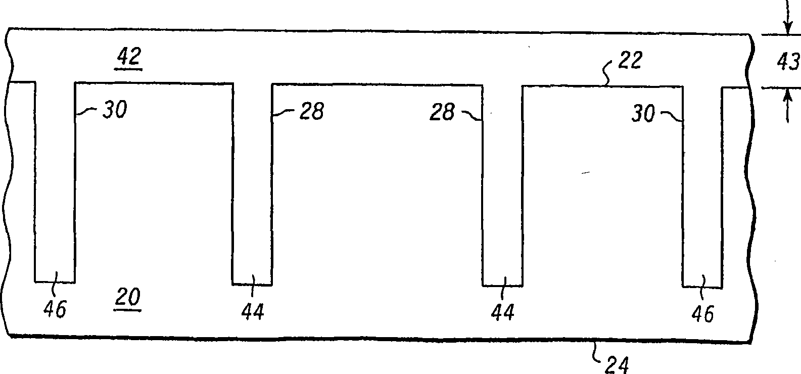
[0025] Figure 1-12 A method of forming a microelectronic assembly including a spiral inductor is shown in accordance with one embodiment of the invention. refer to figure 1 , shows the semiconductor substrate 20 . The semiconductor substrate 20 is made of a semiconductor material such as silicon and includes an upper surface 22 and a lower surface 24 . The thickness of substrate 20 may be approximately 1000 microns. Although only a portion of semiconductor substrate 20 is shown, it should be understood that substrate 20 may be a semiconductor wafer...
PUM
 Abstract
Description
Claims
Application Information