Printed circuit board and method for installing component thereon

A technology of printed circuit boards and components, which is applied to printed circuit parts, printed circuits assembled with electrical components, printed circuits connected with non-printed electrical components, etc., can solve the problem of low utilization of effective area and achieve reduction The effect of surface area and component density

Inactive Publication Date: 2009-10-07
SAMSUNG ELECTRONICS SUZHOU SEMICON
View PDF0 Cites 1 Cited by
  • Summary
  • Abstract
  • Description
  • Claims
  • Application Information

AI Technical Summary

Problems solved by technology

[0006] The purpose of the present invention is to overcome the defects of the low effective area utilization rate of the printed circuit board in the prior art, and provide a printed circuit board mounting structure and a m

Method used


Image

  • Printed circuit board and method for installing component thereon
  • Printed circuit board and method for installing component thereon
  • Printed circuit board and method for installing component thereon

Examples


Example Embodiment

[0015] Hereinafter, embodiments of the present invention will be described in detail with reference to the drawings.

[0016] Refer to figure 2 with image 3 The mounting structure of the printed circuit board and the method of mounting components on the printed circuit board according to the exemplary embodiment of the present invention will be described.

[0017] Refer below image 3 An example of the printed circuit board and the method of mounting components in the printed circuit board according to the embodiment of the present invention will be specifically shown.
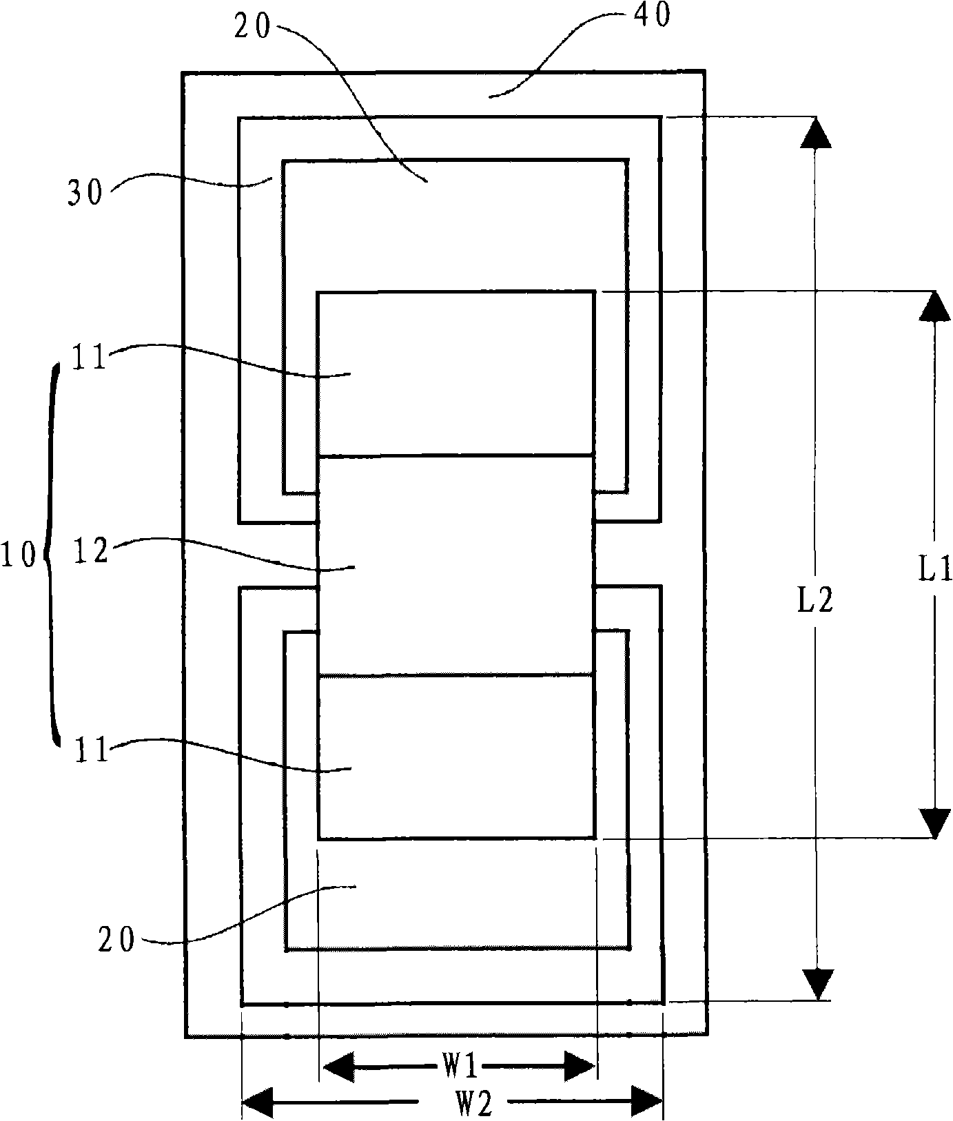
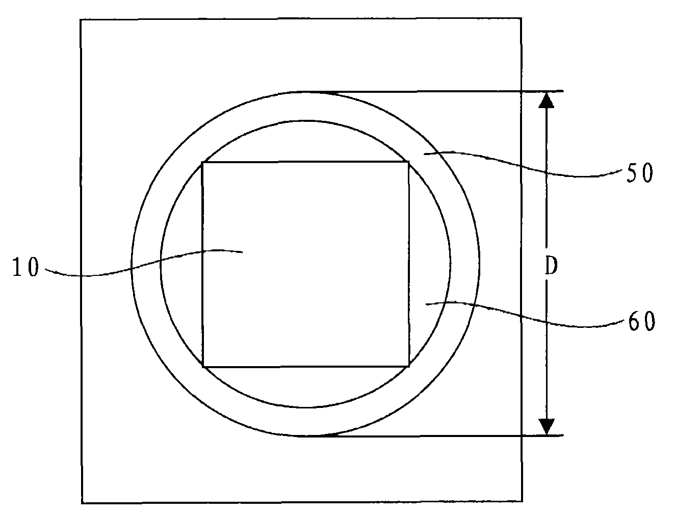
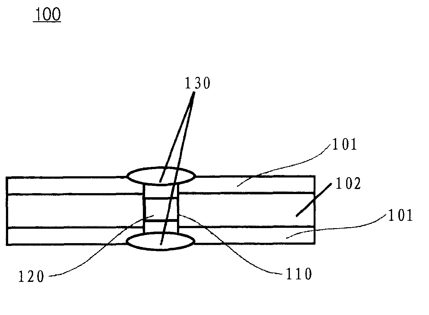
[0018] Refer to image 3 , The printed circuit board 100 includes: a substrate 102 made of an insulating material; a conductive layer 101 formed on the upper and lower surfaces of the substrate 102; at least one through hole 110 formed through the substrate 102 and the conductive layer 101; to be installed The components (for example, resistors, capacitors, exclusions, etc.) 120 are placed vertically in the through...


PUM


Abstract

The invention discloses a printed circuit board and a method for installing a component thereon; the printed circuit board comprises a substrate, conducting layers which are formed on the upper surface and the lower surface of the substrate, at least one through hole which passes through the substrate and the conducting layers, and a component which is arranged in the through hole; the two ends of the component are respectively and electrically connected with the conducting layers formed on the upper surface and the lower surface of the substrate.

Description

technical field [0001] The invention relates to a printed circuit board. More particularly, the present invention relates to a method of mounting components in through-holes of a printed circuit board which reduces the surface area occupied by the components on the printed circuit board. Background technique [0002] With the development of surface mount technology (SMT), the number of components on the surface of the printed circuit board (PCB) is gradually increasing, the density of components is increasing, and the effective use area of ​​the printed circuit board is getting smaller and smaller. [0003] Below, refer to figure 1 To illustrate the surface area occupied by components mounted on a printed circuit board. figure 1 is a mounting method according to the prior art, taking a resistor with a size of 1.0×0.5×0.5 mm (millimeter) as an example, and calculating the surface area of ​​the printed circuit board to be occupied by the resistor mounted on the printed circu...

Claims


Application Information

Patent Timeline
IPC IPC(8): H05K1/02H05K1/18H05K3/34
Inventor 丁飞宇金星
Owner SAMSUNG ELECTRONICS SUZHOU SEMICON
Why Eureka
Try Eureka