Wafer-grade vacuum encapsulation process for micro-electro-mechanical system

A micro-electromechanical system and vacuum packaging technology, which is applied in the process of producing decorative surface effects, decorative arts, micro-structure devices, etc., can solve the problems of small cavity, easy damage, and thin deposited film.

Inactive Publication Date: 2009-10-14
HUAZHONG UNIV OF SCI & TECH
View PDF0 Cites 14 Cited by
  • Summary
  • Abstract
  • Description
  • Claims
  • Application Information

AI Technical Summary

Problems solved by technology

[0004] The invention provides a wafer-level vacuum packaging process for micro-electromechanical systems, which solves the problems of thin deposited films, small cavities,

Method used


Image

  • Wafer-grade vacuum encapsulation process for micro-electro-mechanical system
  • Wafer-grade vacuum encapsulation process for micro-electro-mechanical system
  • Wafer-grade vacuum encapsulation process for micro-electro-mechanical system

Examples


Embodiment 1

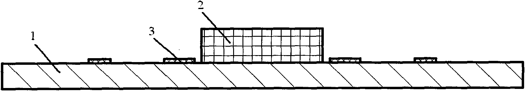
[0032] Deposition getter step: as figure 1 As shown, a Zr-V-Fe getter film 2 is deposited on a silicon substrate 1 by a magnetron sputtering process, and the thickness of the deposited getter film is 50nm, and its shape is two common central bar graph;

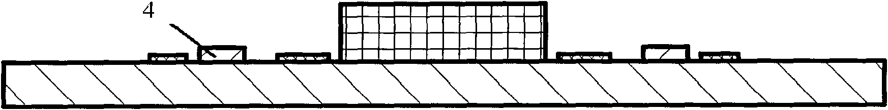
[0033] Step of depositing a thin sacrificial layer: such as figure 2 As shown, a thin sacrificial layer 4 of phospho-silicate glass is deposited on a silicon substrate 1 by a low-pressure chemical vapor deposition process. The thickness of the deposited thin sacrificial layer is 200nm. white space between graphics;

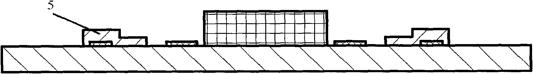
[0034] Deposition buffer cavity sacrificial layer steps: such as image 3 As shown, the sacrificial layer 5 of the phospho-silicate glass buffer cavity is deposited by chemical vapor deposition process, and the thickness of the deposited buffer cavity sacrificial layer is 300nm, and its pattern is made on the edge of the thin sacrificial layer 4 and covers the outer ring getter film;

[0035] Step of depositi...

Embodiment 2

[0041] Deposition getter step: as figure 1 As shown, a Zr-Al getter film 2 is deposited on a silicon substrate 1 by a magnetron sputtering process. The thickness of the deposited getter film is 200 nm, and its shape is two concentric strips surrounding the MEMS device 2. shape graphics;

[0042] Step of depositing a thin sacrificial layer: such as figure 2 As shown, the photoresist is spin-coated on the silicon substrate 1 and the pattern of the thin sacrificial layer 4 is made. The thickness of the deposited thin sacrificial layer is 500nm, and the pattern of the thin sacrificial layer is made in the blank space between the inner and outer circles of the getter thin film patterns. area;

[0043] Deposition buffer cavity sacrificial layer steps: such as image 3 As shown, the photoresist is spin-coated and the buffer chamber sacrificial layer 5 pattern is made. The thickness of the buffer chamber sacrificial layer deposited is 1.5um, and the pattern is made on the edge of th...

Embodiment 3

[0050] Deposition getter step: as figure 1 As shown, a Ti-Mo getter film 2 is deposited on a silicon substrate 1 by a screen printing process. The thickness of the deposited getter film is 200 nm, and its shape is two concentric strips surrounding the MEMS device 2. graphics;

[0051] Step of depositing a thin sacrificial layer: such as figure 2 As shown, a thin sacrificial layer 4 of phospho-silicate glass is deposited on a silicon substrate 1 by a low-pressure chemical vapor deposition process. The thickness of the deposited thin sacrificial layer is 500 nm. white space between graphics;

[0052] Deposition buffer cavity sacrificial layer steps: such as image 3 As shown, the sacrificial layer 5 of the buffer chamber of phospho-silicate glass is deposited by chemical vapor deposition process, and the thickness of the deposited buffer chamber sacrificial layer is 1.5um, and its pattern is made on the edge of the thin sacrificial layer 4 and covers the outer ring getter fi...


PUM

PropertyMeasurementUnit
Thicknessaaaaaaaaaa
Thicknessaaaaaaaaaa
Thicknessaaaaaaaaaa

Abstract

A wafer-grade vacuum encapsulation process for a micro-electro-mechanical system belongs to an encapsulation method for a micro-electro-mechanical system and solves the problems of the film deposition-based vacuum encapsulation process that the deposited film is thin, has small chamber and is easy to be damaged and the encapsulation device has leaked vacuum and reduced service life. The process sequentially comprises a step of depositing an air absorbent, a step of depositing a thin sacrificial layer, a step of depositing a cushion chamber sacrificial layer, a step of depositing thick sacrificial layer, a step of preparing an encapsulation cover, a step of etching a releasing hole, a step of removing sacrificial layer and a step of sealing. The process solves the problems that the existing encapsulation method has short vacuum retaining time, low sealing quality, large encapsulation dimension, incompatibility between the process and the standard IC process and high cost, thus ensuring the air pressure in the inner-most chamber; and simultaneously, the cost of the process is less than that of the vacuum encapsulation based on wafer-bonding process, and the process can realize production in general IC production factories and greatly promote the development and generalization of wafer-grade MEMES vacuum encapsulation technology.

Description

technical field [0001] The invention belongs to a micro-electro-mechanical system packaging method, in particular to a wafer-level vacuum packaging process for a micro-electro-mechanical system. Background technique [0002] Microelectromechanical systems (MEMS) devices such as absolute pressure sensors, inertial sensors based on resonance principles (such as accelerometers, angular velocity sensors, gyroscopes), micro-vacuum electronic devices and optical devices (optical switches, infrared imaging sensors, digital micromirror devices) , need to work in a specific vacuum environment, these devices need vacuum packaging. Vacuum packaging can be divided into device-level vacuum packaging and wafer-level vacuum packaging. Wafer-level vacuum packaging has the advantages of low cost, high output, and guaranteed dicing safety, and has important application prospects. At present, MEMS wafer-level vacuum packaging mainly adopts two technical routes: the vacuum packaging method ba...

Claims


Application Information

Patent Timeline
IPC IPC(8): B81C1/00
Inventor 汪学方黎藜张卓刘川甘志银张鸿海刘胜
Owner HUAZHONG UNIV OF SCI & TECH
Why Eureka
Try Eureka