LTCC-based CGA integrated packaging structure and realization method thereof

A technology of packaging structure and implementation method, which is applied in the direction of electric solid-state devices, semiconductor devices, semiconductor/solid-state device components, etc., can solve the problems of low system integration density, large edge space, and low packaging efficiency, so as to improve system integration density , High I/O port density, the effect of meeting the design requirements

Active Publication Date: 2017-10-27
XIAN INSTITUE OF SPACE RADIO TECH
View PDF10 Cites 17 Cited by
  • Summary
  • Abstract
  • Description
  • Claims
  • Application Information

AI Technical Summary

Problems solved by technology

The packaging structure has the following defects: passive components cannot be integrated, and the system integration density is low; HTCC line resistance is large, and the signal voltage drop is large; HTCC material properties cannot be applied to high frequency fields; HTCC shrinkage consistency is poor, as To ensure good welding of the metal frame, a large edge space needs to be left, and the sidewall width increases with the increase in size, resulting in low packaging efficiency

Method used


Image

  • LTCC-based CGA integrated packaging structure and realization method thereof
  • LTCC-based CGA integrated packaging structure and realization method thereof
  • LTCC-based CGA integrated packaging structure and realization method thereof

Examples


Embodiment Construction

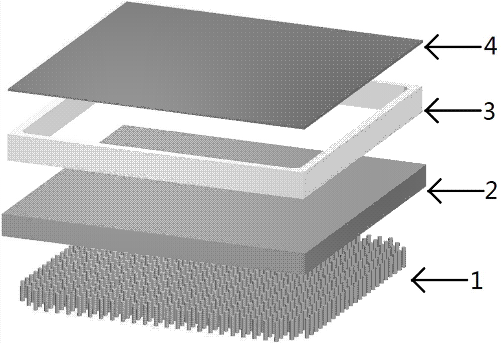
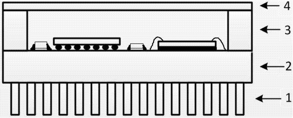
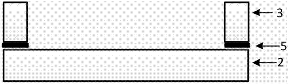
[0046] like figure 1 As shown, the packaging structure of the present invention includes a CGA array 1 , an LTCC substrate 2 , a surrounding frame 3 and a cover plate 4 . The frame 3 is welded on the upper surface of the LTCC substrate 2 , the CGA array 1 is welded on the bottom surface of the LTCC substrate 2 , the LTCC substrate 2 is electrically and mechanically interconnected with the lower PCB through the CGA array 1 , and the cover plate 4 is welded on the frame 3 . The upper surface of the LTCC substrate 2 is used for assembling components.

[0047] The LTCC substrate 2 is a plane structure with n blind cavities on the plane, where n is a natural number.

[0048] The surrounding frame 3 and the cover plate 4 are made of metal, preferably iron-nickel alloy.

[0049]The thickness of the LTCC substrate 2 is not less than 2 mm, the height of the frame 3 is not less than 3 mm, and the contact width between each edge of the frame 3 and the LTCC substrate 2 is 2 mm.

[0050...


PUM


Abstract

The invention discloses an LTCC-based CGA integrated packaging structure and a realization method thereof. An LTCC technology and a CGA technology are combined, and a CGA array is manufactured on the bottom surface of an LTCC substrate by adopting a tool through a welding mode; the LTCC is used as an interconnecting substrate, a packaging body and a passive element integrated carrier of the module at the same time; and the whole region or a partial region on the substrate is welded with a metal surrounding frame, and airtight packaging in the metal surrounding frame region can be realized through parallel seam welding or laser melting seaming ways. The packaging structure is mainly used for the field of system integration as a packaging platform; by adoption of the CGA, high-reliability interconnection between the module and the exterior is realized, so that large module packaging dimensions can be realized; by adoption of the LTCC, integration of active devices and passive elements can be realized at the same time, so that system integrated density is greatly improved; by virtue of the high-precision welding of the metal surrounding frame, high packaging efficiency is realized; due to the position and shape changes of the metal surrounding frame, different applications of electromagnetic shielding, airtightness and the like can be realized; and in addition, the packaging structure has high fundamentality and expandability.

Description

technical field [0001] The invention relates to an LTCC-based CGA integrated packaging structure and a realization method thereof, and belongs to the field of system integrated packaging of electronic products. Background technique [0002] The current main structure of the digital processing circuit is to assemble the discrete packaged chips on the PCB board using SMT technology. However, with the requirements of miniaturization, light weight and high reliability of the product, the conventional process installation method has been difficult to meet the product requirements. [0003] Secondary integration of multiple bare chips or chip-level packaged chips, packaging multiple VLSI (bare chips) and passive components into one package at one time, can greatly reduce the system volume and improve the system performance. reliability, simplify thermal design of the system, and simplify PCB assembly. [0004] The currently commonly used packaging structure is the HTCC integrated...

Claims


Application Information

Patent Timeline
Patent Type & Authority Applications(China)
IPC IPC(8): H01L23/31H01L25/11
CPCH01L23/3121H01L25/115H01L2224/16225H01L2224/48091H01L2224/73265H01L2924/19105H01L2924/00014
Inventor 石伟张婷张保王宏王升赵雅
Owner XIAN INSTITUE OF SPACE RADIO TECH
Why Eureka
Try Eureka