

Lead cutter and method of cutting lead
A cutter and lead wire technology, applied in the direction of electrical solid devices, semiconductor devices, semiconductor/solid device manufacturing, etc., can solve problems such as insufficient and achieve high reproducibility effects
- Summary
- Abstract
- Description
- Claims
- Application Information
AI Technical Summary
Problems solved by technology
Method used
Image

Examples
no. 1 example
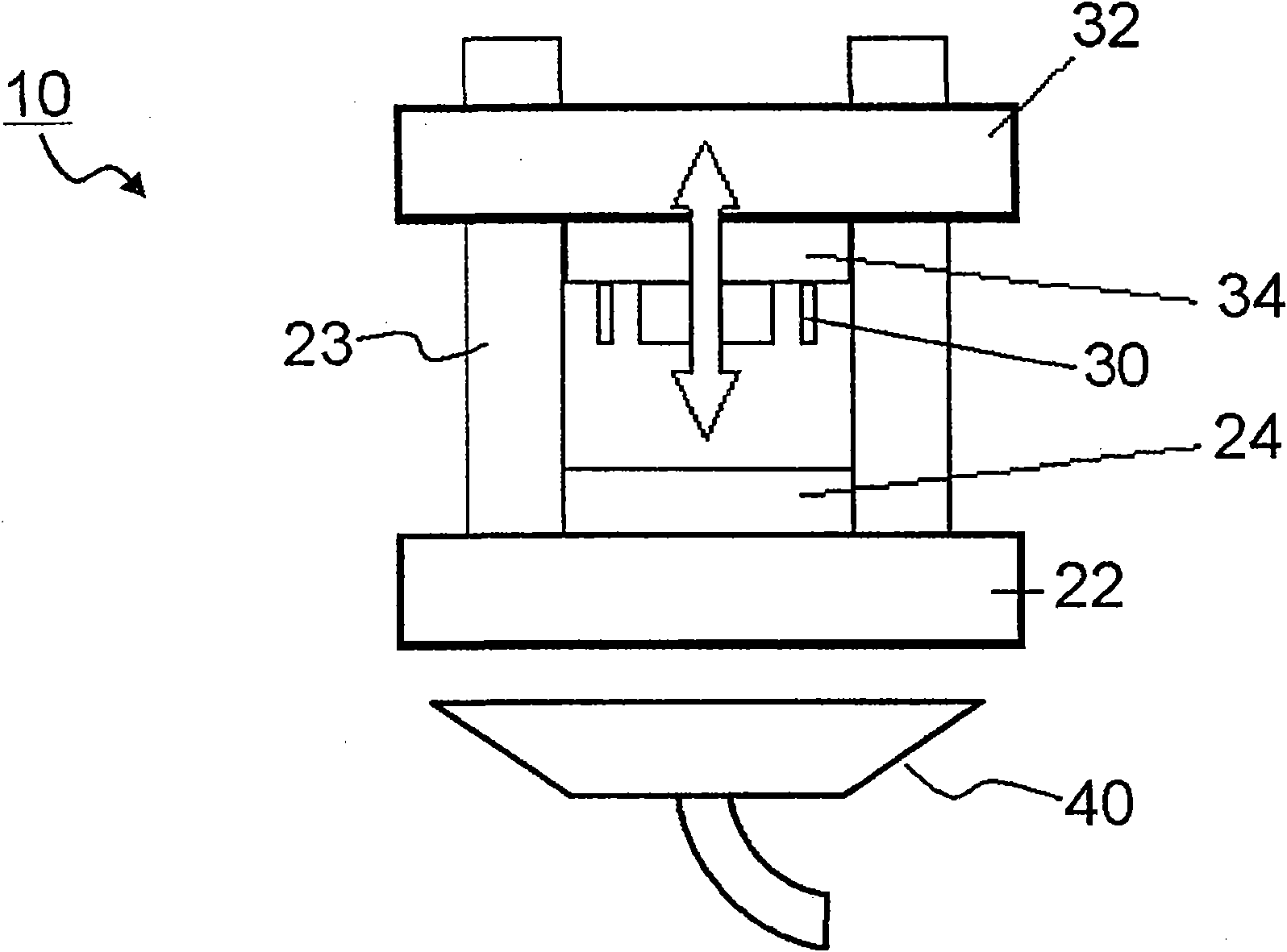
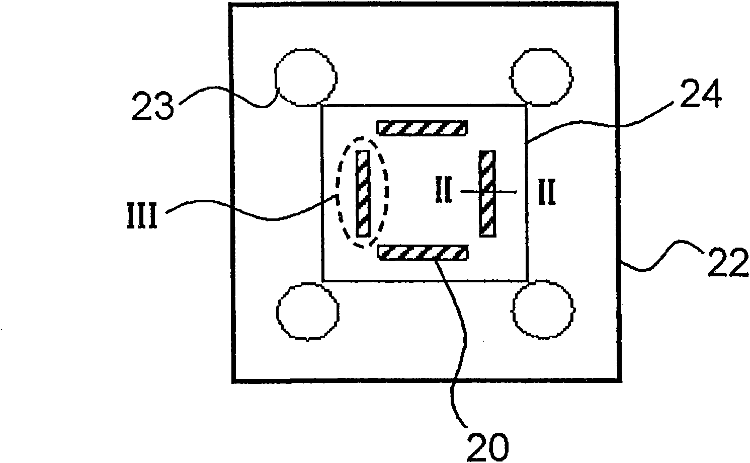
[0041] Figure 1A is a schematic side view showing the wire cutter according to this embodiment, and Figure 1B is a schematic plan view of the lower die device constituting the lead cutter.
[0042] figure 2 is a schematic vertical sectional view showing a punch and a die of a wire cutter according to this embodiment (hereinafter, the combination of a punch and a die is referred to as a function executing unit as the case may be) and its corresponds to along Figure 1B A cross-sectional view taken along line II-II. image 3 is a schematic plan view of the functional execution unit, and it corresponds to Figure 1B Region III enclosed by the dashed line in . Figure 4 is a schematic vertical sectional view showing the function executing unit in a state where the ventilator is activated. Figure 5A is a schematic plan view showing a semiconductor chip having leads to be cut by the lead cutting method according to the first embodiment, and Figure 5B is along Figure 5A A...
no. 2 example
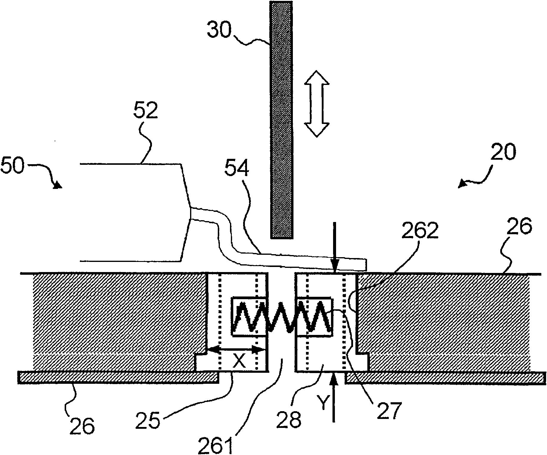
[0120] Figure 6 is a schematic vertical sectional view showing the function executing unit of the wire cutter 10 according to this embodiment. In the wire cutter 10 according to this embodiment, the blade portion 25 is finished in black, and the temperature controller includes a light source 42 that emits light toward the blade portion 25 . Increasing and decreasing the amount of light emitted by the light source 42 can control the amount of heat radiated to the blade portion 25 . Therefore, the temperature of the blade portion 25 can be controlled to adjust the cutting gap as desired.
[0121] The light source 42 may be constituted by an illuminator or LED emitting visible light or infrared rays.
[0122] The wire cutter 10 according to this embodiment may include both the light source 42 and the ventilation device 40 . In this case, heating by light source 42 and cooling by ventilation device 40 can be performed as desired. Therefore, the selection range for setting the...
no. 3 example
[0131] In the wire cutter 10 according to this embodiment, the temperature control of the punch 30 and the die 20 is automatically performed by the temperature controller so as to accurately realize the cutting gap specified by the user.
[0132] Specifically, the wire cutter 10 according to this embodiment holds a memory of the cutting gap therebetween and the output of the ventilation device 40 obtained when the stamper 20 and the punch 30 reach the equilibrium temperature. Likewise, the wire cutter 10 includes an output control that increases and decreases the output of the ventilation device 40 to achieve the cutting gap specified by the user.
[0133] The output of the ventilation device 40 and the corresponding cutting gap are stored in the memory unit of the wire cutter 10 in the form of a calibration curve, a table or a function.
[0134] The wire cutter 10 according to this embodiment controls the temperature of the stamper 20 and the punch 30 through the output contr...
PUM
| Property | Measurement | Unit |
|---|---|---|
| thickness | aaaaa | aaaaa |
| width | aaaaa | aaaaa |
Abstract
Description
Claims
Application Information