A black conductive paste composition, an anti-electromagnetic wave filter comprising the composition and a display
A technology of anti-electromagnetic wave and composition, which is applied in the direction of conductive materials, conductive materials, conductive materials dispersed in non-conductive inorganic materials, etc., can solve the problems of partial open circuit or short circuit, stained line width, decrease of appearance characteristics of plasma display, etc.
- Summary
- Abstract
- Description
- Claims
- Application Information
AI Technical Summary
Problems solved by technology
Method used
Image

Examples
Embodiment 1-4 and comparative example 1-2
[0122] According to the components and contents shown in Table 1 below, mix the acrylate polymer resin with monomer or oligomer, solvent, glass powder, conductive metal, black pigment and dispersant, stir at room temperature, and finally use three rollers to (3-roll) mill (mill), to manufacture the required black conductive paste composition for gravure offset printing.
[0123] [Table 1]
[0124]
[0125]In Table 1, the weight-average molecular weight of acrylate polymer resin is 15000, which is composed of methyl acrylate (methyl acrylate, MA), butyl methacrylate (butyl methacrylate, BM), hydroxyethyl methacrylate (hydroxyl ethyl methacrylate (HEMA) and methylmethacrylate (methylmethacrylate, MMA) are formed by copolymerization in parts by weight of 30:40:10:20, respectively.
[0126] Also, A is urethane acrylate, B is trimethylolpropane triacrylate modified ethylene oxide, C is trimethylolpropane triacrylate modified propylene oxide, and D is bisphenol A ethoxylated Di...
experiment example
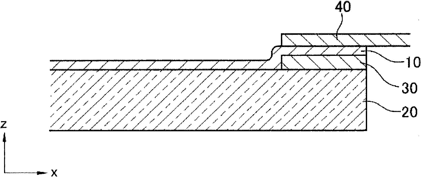
[0129] Form anti-electromagnetic wave filter
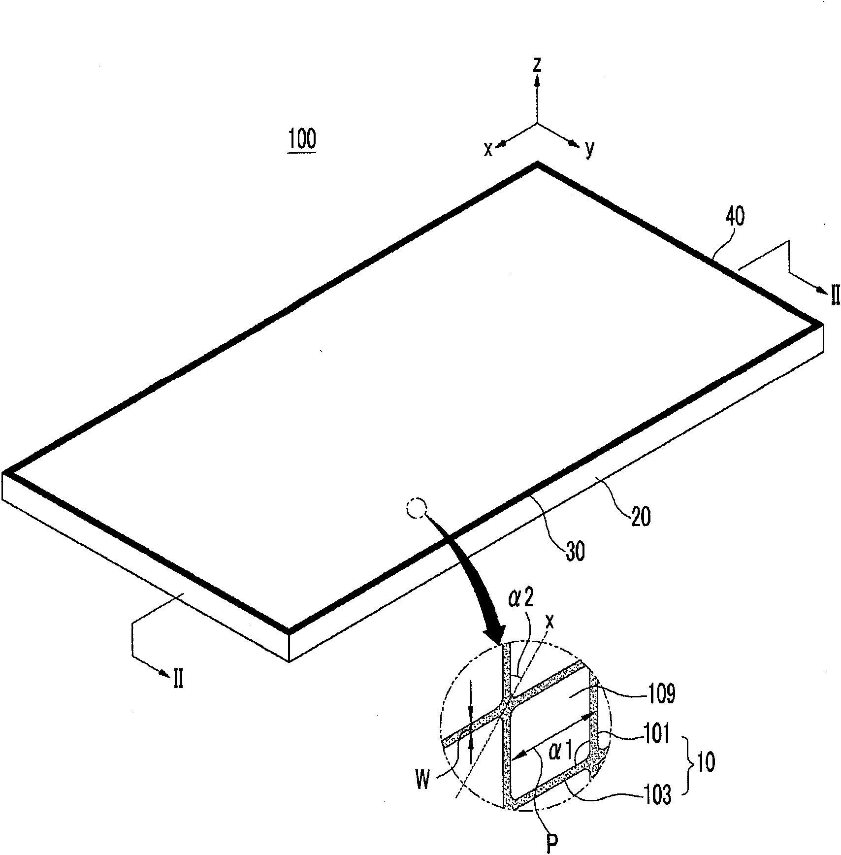
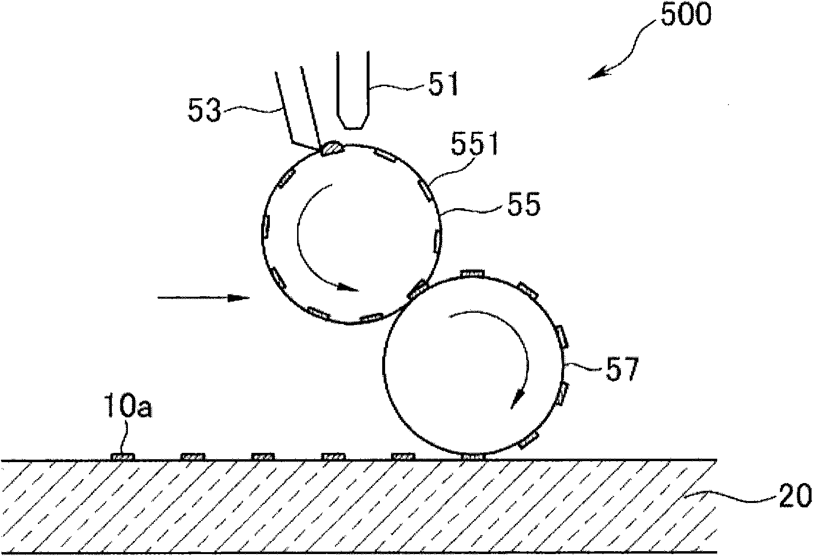
[0130] By using the paste compositions prepared in Examples 1 to 4 and Comparative Examples 1 and 2, gravure offset printing was performed according to the pattern specification for the electromagnetic wave shielding filter.
[0131] i.e. by and as image 3 The same offset printing apparatus as shown, prints the paste composition onto a glass substrate to form a screen-like pattern. At this time, the line width of the mesh-like patterns is 30 μm, and the standard average pitch of the patterns is 300 μm.
[0132] Then, in the firing process, the paste composition is kept on the glass substrate for 20 minutes at a temperature of 500-540° C. to form a mesh pattern for an electromagnetic wave filter.
[0133] Characteristic evaluation of anti-electromagnetic wave filter
[0134] The dispersibility, printability and dryness of the anti-electromagnetic wave filter prepared using the paste compositions provided in Examples 1-4 and...
PUM
| Property | Measurement | Unit |
|---|---|---|
| The average particle size | aaaaa | aaaaa |
| Average spacing | aaaaa | aaaaa |
| Width | aaaaa | aaaaa |
Abstract
Description
Claims
Application Information
 - R&D Engineer
- R&D Manager
- IP Professional
- Industry Leading Data Capabilities
- Powerful AI technology
- Patent DNA Extraction
Browse by: Latest US Patents, China's latest patents, Technical Efficacy Thesaurus, Application Domain, Technology Topic.
© 2024 PatSnap. All rights reserved.Legal|Privacy policy|Modern Slavery Act Transparency Statement|Sitemap