

Manufacturing method for optical waveguide module
A technology of optical waveguide and manufacturing method, which is applied to the coupling of optical waveguide, optical waveguide light guide, light guide, etc., can solve the problems of insufficient precision, large optical L coupling loss, and easy deviation of cut surface accuracy, etc., to achieve improvement Production efficiency and the effect of reducing the coupling loss of light
- Summary
- Abstract
- Description
- Claims
- Application Information
AI Technical Summary
Problems solved by technology
Method used
Image

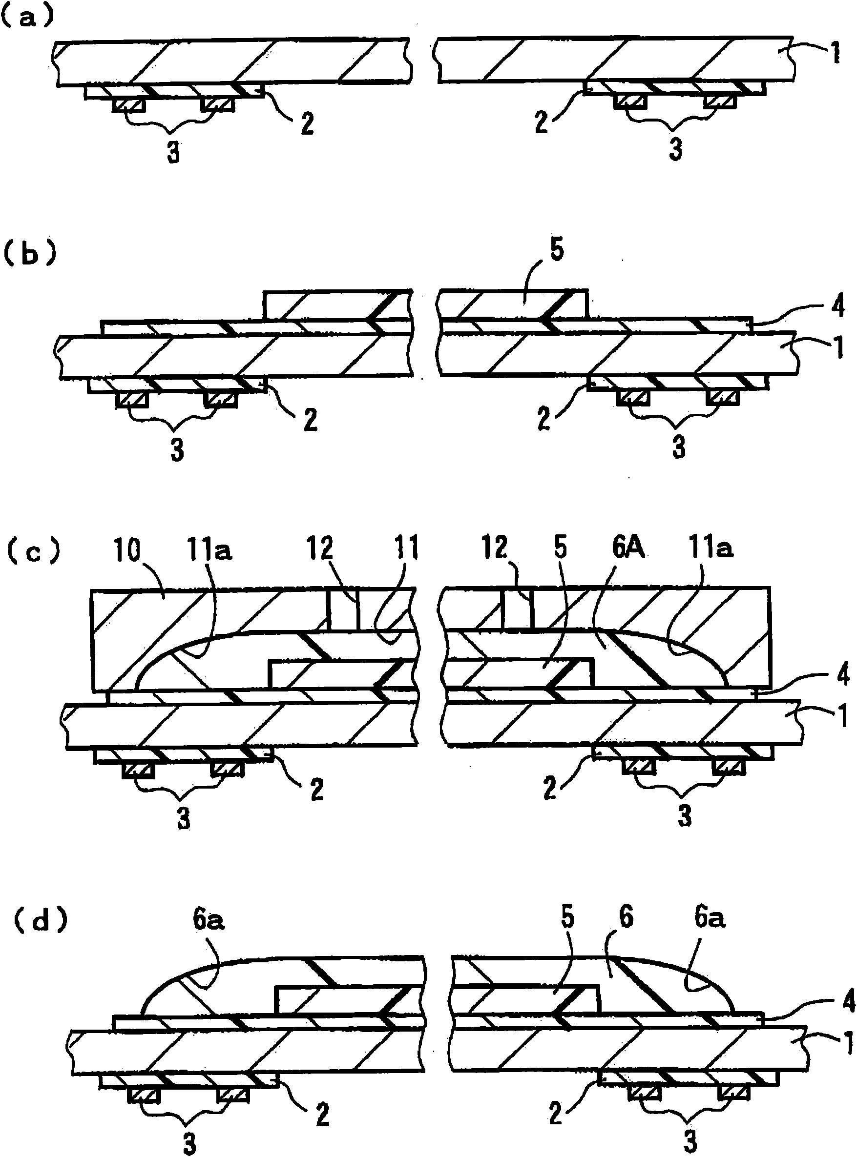
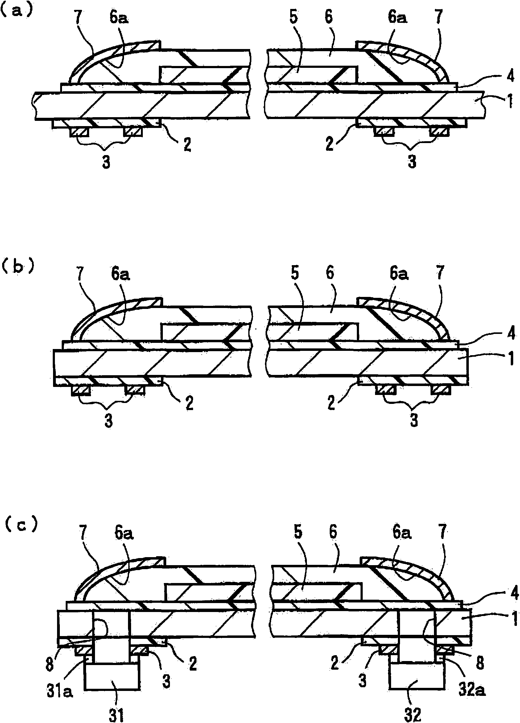
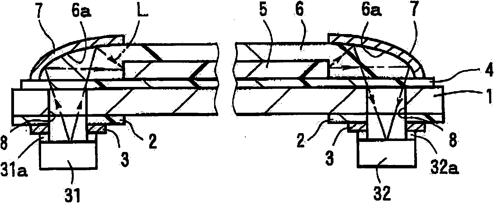
Examples
Embodiment
[0053] Materials for forming the under cladding layer and the over cladding layer
[0054] Mix 35 parts by weight of bisphenoxyethanol fluorenyl glycidyl ether (component A) represented by the following general formula (1), and 40 parts by weight of alicyclic epoxy resin, that is, 3',4'-epoxy ring Hexylmethyl 3,4-epoxyethylene carboxylate (manufactured by Daicel Chemical Industry Co., Ltd., Celloxide 2021P) (component B), 25 parts by weight of alicyclic epoxy resin (Daicel Manufactured by Chemical Industry Co., Ltd., Celloxide 2081) (component C), 2 parts by weight of 4,4'-bis[bis(β-hydroxyethoxy)phenylsulfite]phenylsulfate-bis-hexafluoroantimonate A 50% propylene carbonate solution (component D) was prepared as a material for forming the under cladding layer and the over cladding layer.
[0055] Chemical 1
[0056]
[0057] (wherein, R1~R6 are hydrogen atoms, n=1)
[0058] core forming material
[0059] 70 parts by weight of the above component A, 30 parts by wei...
PUM
 Abstract
Description
Claims
Application Information