Chip encapsulation structure and support device thereof
A chip packaging and supporting device technology, applied in semiconductor/solid-state device parts, semiconductor devices, electrical components, etc., can solve problems such as uneven surface, inability to solve thin-film flip-chip packaging, and inability to solve the problem of chip packaging structure, etc. Avoid wrinkle effect
- Summary
- Abstract
- Description
- Claims
- Application Information
AI Technical Summary
Problems solved by technology
Method used
Image


Examples
Embodiment Construction
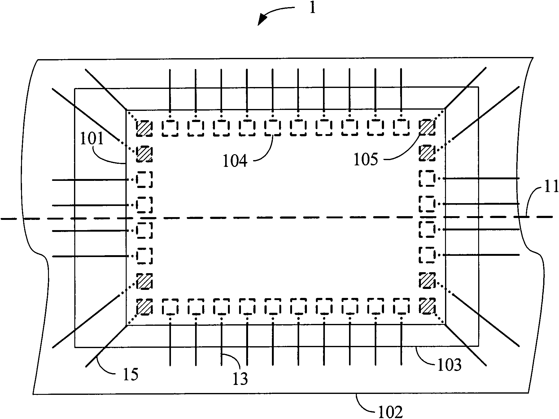
[0022] The invention relates to a chip packaging structure and its supporting device. Specifically, the chip package structure of the present invention includes a chip, a flexible substrate, and a supporting device, wherein, the central part of the active surface of the chip has a sensing area for sensing information to be introduced from the outside, such as fingerprints . The present invention utilizes the supporting device so that the flexible substrate on which the chip is placed can still maintain a preset flatness after packaging, so that the sensing area can still operate accurately after packaging. The following examples are used to illustrate the content of the present invention, but not to limit the present invention. It should be noted that in the following embodiments and drawings, the components irrelevant to the present invention have been omitted and not shown; and for the sake of easy understanding, the size ratio between the components is drawn exaggeratedly,...
PUM
 Abstract
Description
Claims
Application Information