Manufacturing method of opto-electric hybrid board

A technology of optoelectronic mixing and manufacturing method, which is applied in the manufacturing of printed circuits, coupling of optical waveguides, optics, etc., can solve the problems of increasing the loss of optical L coupling, and achieve the effect of small coupling loss of light

Active Publication Date: 2009-10-28
NITTO DENKO CORP
View PDF1 Cites 24 Cited by
  • Summary
  • Abstract
  • Description
  • Claims
  • Application Information

AI Technical Summary

Problems solved by technology

In this state, the light L propagates in a state where the optical axes of the light-emitting element 11 and the light-receiving element 12 are shifted relative to the optical path conversion mirrors 87a at both ends of the core 87, and the coupling loss of the light L becomes large.

Method used


Image

  • Manufacturing method of opto-electric hybrid board
  • Manufacturing method of opto-electric hybrid board
  • Manufacturing method of opto-electric hybrid board

Examples


Embodiment

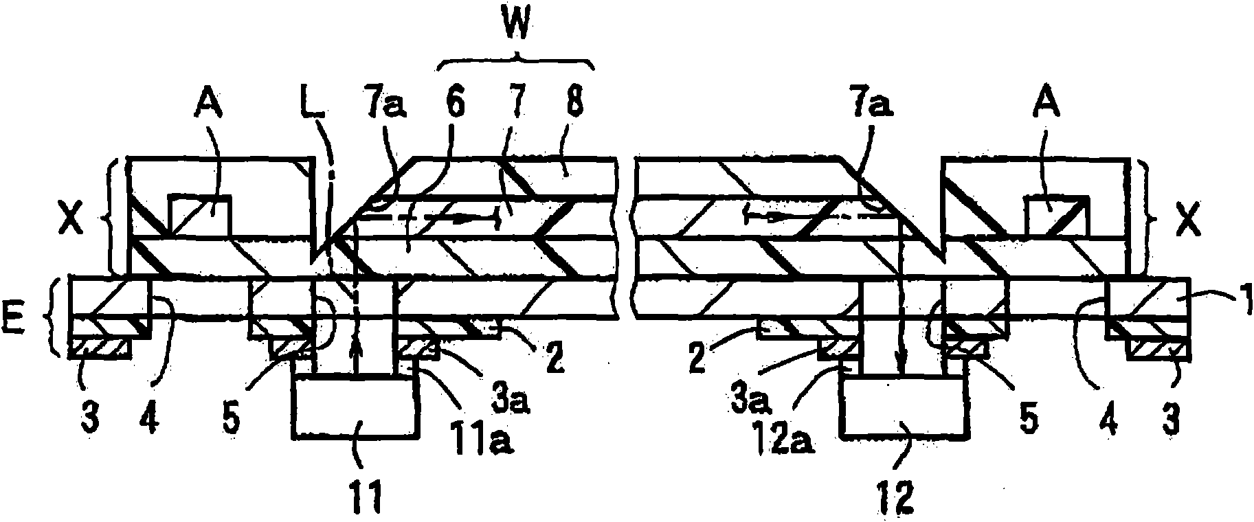
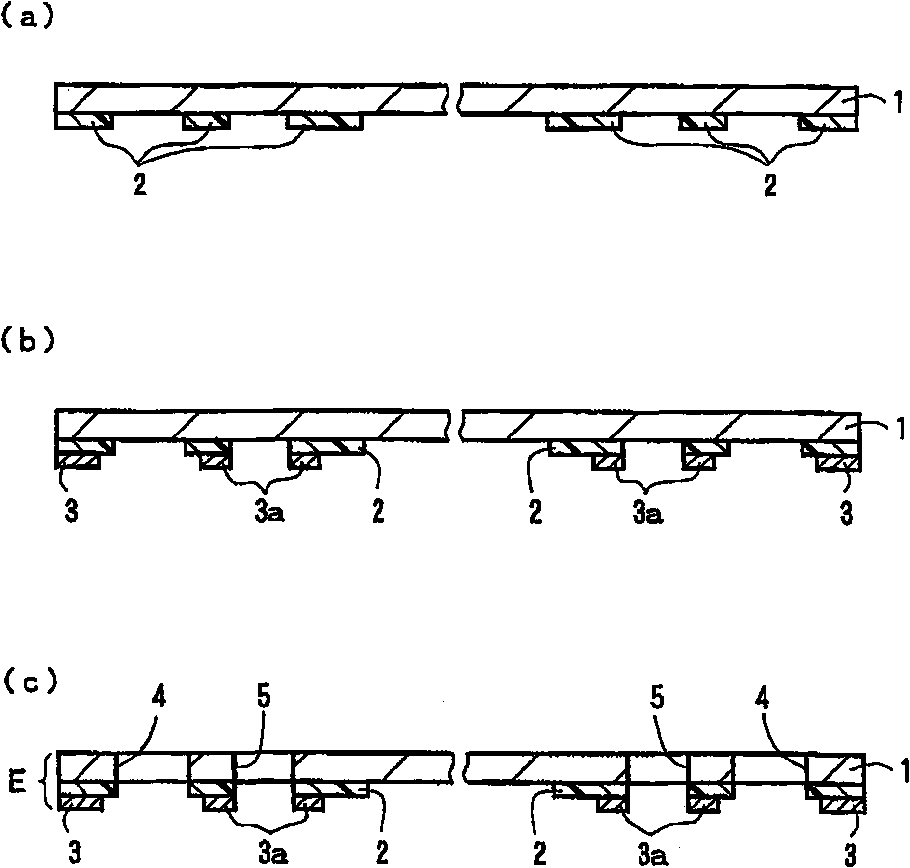
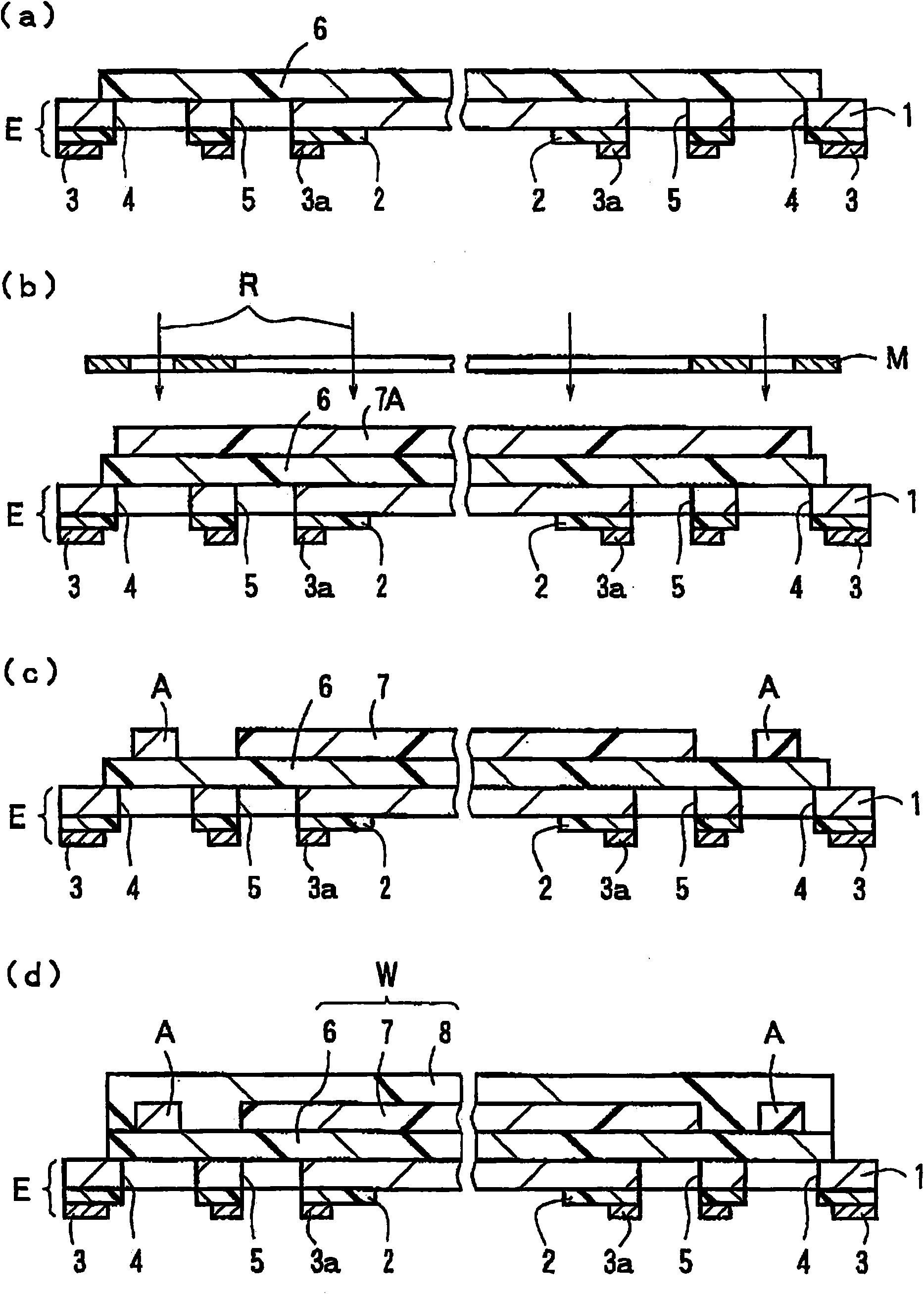
[0042] Formation of circuit board

[0043] On one surface of a stainless steel substrate (SUS304 foil with a thickness of 20 μm), first, an insulating layer (10 μm in thickness) made of a photosensitive polyimide resin was formed into a predetermined pattern by photolithography. Next, a seed layer made of a copper / nickel / chrome alloy was formed on the front surface of the insulating layer by sputtering. Next, after a dry thin film resist was pasted on both surfaces of the laminate composed of the above-mentioned stainless steel substrate, insulating layer, and seed layer, on the above-mentioned dry thin film resist on the side where the above-mentioned seed layer was formed, , using a photolithography method to form a groove portion of a circuit pattern including a mounting pad, and to expose the front surface portion of the seed layer at the bottom of the groove portion. Next, an electrolytic copper plating layer (thickness: 20 μm) was laminated and formed on the front sur...


PUM


Abstract

An opto-electric hybrid board manufacturing method improves the alignment accuracy of an optical element with respect to a core of an optical waveguide. When a core (7) of an optical waveguide (W) is formed on a surface of an electric circuit board (E), the core (7) and optical element positioning alignment marks (A) are simultaneously formed from a photosensitive resin layer including a core formation region and an alignment mark formation region by a single photolithography process. In an optical element mounting step, a light emitting element (11) and a light receiving element (12) are mounted at proper positions with respect to the core (7) of the optical waveguide (W) with reference to the alignment marks (A).

Description

technical field [0001] The present invention relates to a method of manufacturing an optoelectronic hybrid board on which an optical waveguide and a circuit on which an optical element is mounted are combined. Background technique [0002] Conventionally, the photoelectric hybrid board is formed by separately manufacturing the circuit board and the optical waveguide, and bonding the circuit board and the optical waveguide with an adhesive. For example, if Figure 6 As shown, the above-mentioned photoelectric hybrid substrate is formed as follows: on the circuit substrate 81 on which the multilayer circuit 83 is formed, an optical circuit composed of a lower cladding layer 86, a core 87, and an upper cladding layer 88 is adhered with high precision by means of an adhesive 82. Waveguide 80. Furthermore, the light-emitting element 11 and the light-receiving element 12 are flip-chip mounted on mounting pads (a part of the circuit 83 ) formed on the circuit board 81 (for example...

Claims


Application Information

Patent Timeline
Patent Type & Authority Applications(China)
IPC IPC(8): G02B6/13
CPCG02B6/13H05K3/0023H05K1/0269G02B6/4214G02B6/43H05K1/0274H05K2201/09918G02B6/4224G02B6/42G02B6/12
Inventor 程野将行
Owner NITTO DENKO CORP
Why Eureka
Try Eureka