Wafer fixing device and wafer fixing method

A wafer fixation and wafer technology, which is applied in semiconductor/solid-state device manufacturing, electrical components, circuits, etc., can solve problems such as limited space utilization, poor wafer flatness, and reduced process design flexibility. Flexibility and space utilization, improve the reliability of flatness, and save the time of production replacement

Inactive Publication Date: 2009-11-11
MICROELECTRONICS TECH INC
View PDF1 Cites 9 Cited by
  • Summary
  • Abstract
  • Description
  • Claims
  • Application Information

AI Technical Summary

Problems solved by technology

However, the structure of the loading table in US 6,803,780 is a solid structure. The loading table is only used to carry and fix the semiconductor wafer, and it is impossible to install test components under the wafer. If it is used in the process of light-emitting diodes, it cannot be placed on the loading table The thimbler is placed in the middle to sort the die, so its space utilization is limited, and it is impossible to install test components under the wafer during the wafer process flow, which reduces the flexibility of the process design.
[0005]Therefore, there is still a need for a device or system that can solve the above-mentioned distorted grain arrangement, poor wafer flatness and poor space utilization, so as to improve Production pass rate

Method used


Image

  • Wafer fixing device and wafer fixing method
  • Wafer fixing device and wafer fixing method
  • Wafer fixing device and wafer fixing method

Examples


Embodiment Construction

[0040] In order to enable those skilled in the art to better understand the solution of the present invention, and to make the above-mentioned purpose, features and advantages of the present invention more obvious and comprehensible, the present invention will be further described in detail below in conjunction with the accompanying drawings and embodiments.

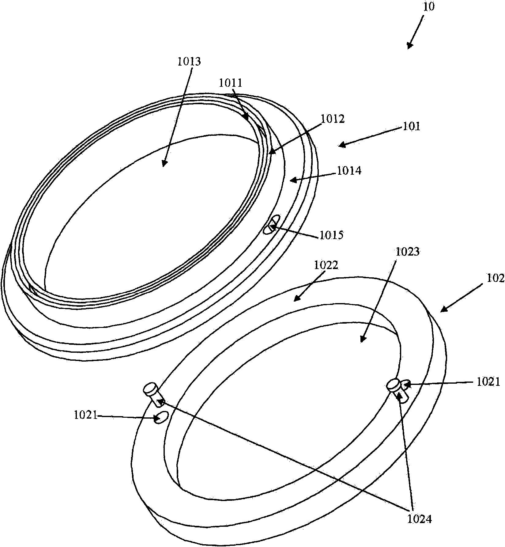
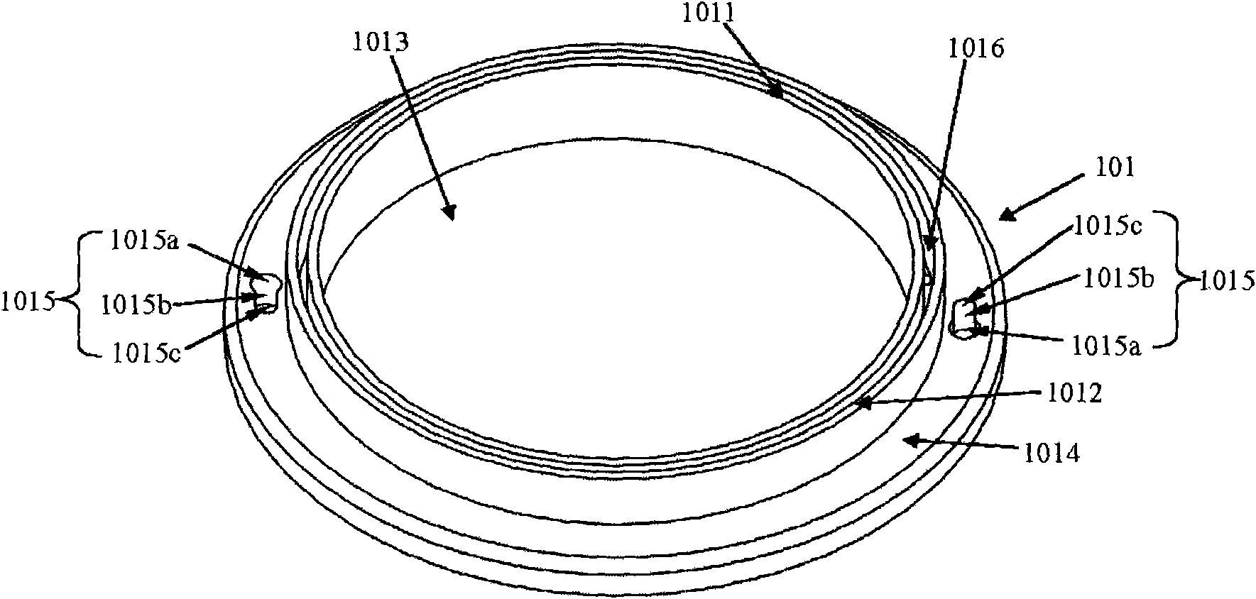
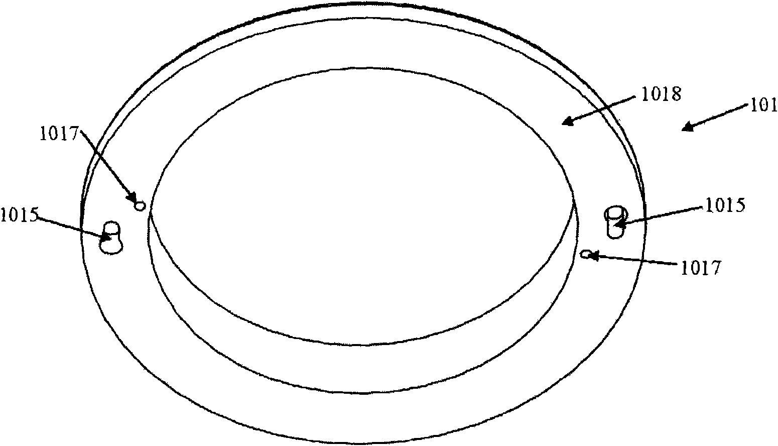
[0041] The invention provides a wafer fixing device, which can fix the blue film carrying the wafer by means of vacuum adsorption. Such as figure 1 As shown, in a preferred embodiment of the present invention, the wafer fixing device 10 includes a wafer fixing ring 101 and an adsorption device 102, and the wafer fixing ring 101 and the adsorption device 102 hold the wafer fixing ring 101 by a snap-fitting device. fixed on the adsorption device 102. The wafer fixing ring 101 includes an inner ring 1011 , an outer ring 1012 and an annular base portion 1014 . In one embodiment, the inner ring 1011 , the outer ring 1012 an...


PUM


Abstract

The invention discloses a wafer fixing device and a wafer fixing method, which are used for solving the problems of twisted crystal grain arrangement, poor wafer flatness and poor space usage rate in the prior art. The wafer fixing device comprises a vacuum source, an adsorption device and a wafer fixing ring, wherein a first through hole is formed in the adsorption device, and the first through hole is connected to the vacuum source; the wafer fixing ring is arranged on the adsorption device and is fixed on the adsorption device through a clamping device; and the wafer fixing ring comprises an inner ring, an outer ring and an annular base, wherein the inner ring and the outer ring are formed on the annular base, an adsorption space is formed between the inner ring and the outer ring, and the annular base comprises a second through hole which is used for connecting the first through hole and the adsorption space. The wafer fixing method comprises the following steps: preparing the adsorption device; putting the wafer fixing ring on the adsorption device, and then, clamping the wafer fixing ring and the adsorption device through the clamping device; forming a vacuum state in the wafer fixing ring and the adsorption device; and putting a blue film pasted with a wafer on the wafer fixing ring.

Description

technical field [0001] The invention relates to a wafer fixing device, in particular to a wafer fixing device utilizing vacuum adsorption and a method thereof. Background technique [0002] Light emitting diodes (Light emitting diodes, LEDs) are becoming more and more widely used. At present, multiple light emitting diodes are arranged in arrays to present applications of light sources or displays; and on the wafer of the same light emitting diode, the color between the grains The wavelength and brightness are different. In order to meet the consistency of the product's requirements for color wavelength and brightness sensitivity, it is necessary to perform a crystal-picking process on the LED grains in the process steps. Before the die-picking process step, the LED wafer needs to be adhered to the blue film to fix the die when the wafer is divided into die. Afterwards, it is necessary to expand the blue film and use the expansion ring to be fixed on the edge of the blue f...

Claims


Application Information

Patent Timeline
IPC IPC(8): H01L21/683
Inventor 张介舟廖洪佐林学宏张志安
Owner MICROELECTRONICS TECH INC
Why Eureka
Try Eureka