DA converter circuit, liquid crystal driver circuit, liquid crystal display apparatus, and method for designing DA converter circuit
A technology for transforming circuits and liquid crystal display panels, applied to electrical components, code conversion, static indicators, etc., can solve problems such as the inability to eliminate the deviation between the output gray-scale voltage and the ideal gray-scale voltage, so as to prevent the degradation of display quality and prevent Shows the effect of degraded quality
- Summary
- Abstract
- Description
- Claims
- Application Information
AI Technical Summary
Problems solved by technology
Method used
Image
Examples
Embodiment approach 1
[0068] Refer below Figure 1 to Figure 8 , Embodiment 1 of the present invention will be described.
[0069] (Structure of Liquid Crystal Display Device 10)
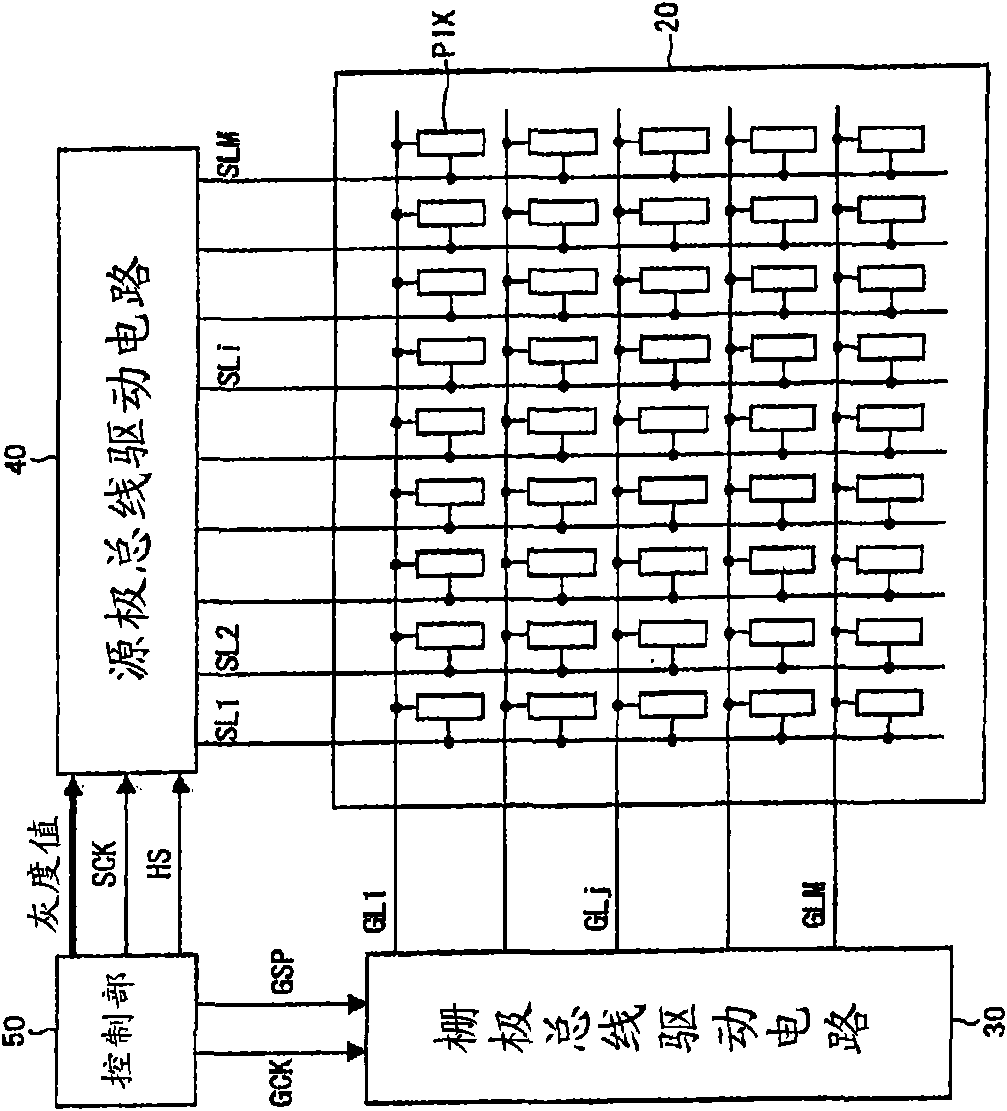
[0070] First, refer to figure 2 , the structure of the liquid crystal display device 10 of the present invention will be described. figure 2 It is a block diagram showing the configuration of a TFT (Thin Film Transistor) type liquid crystal display device 10 which is a representative example of the active matrix type.
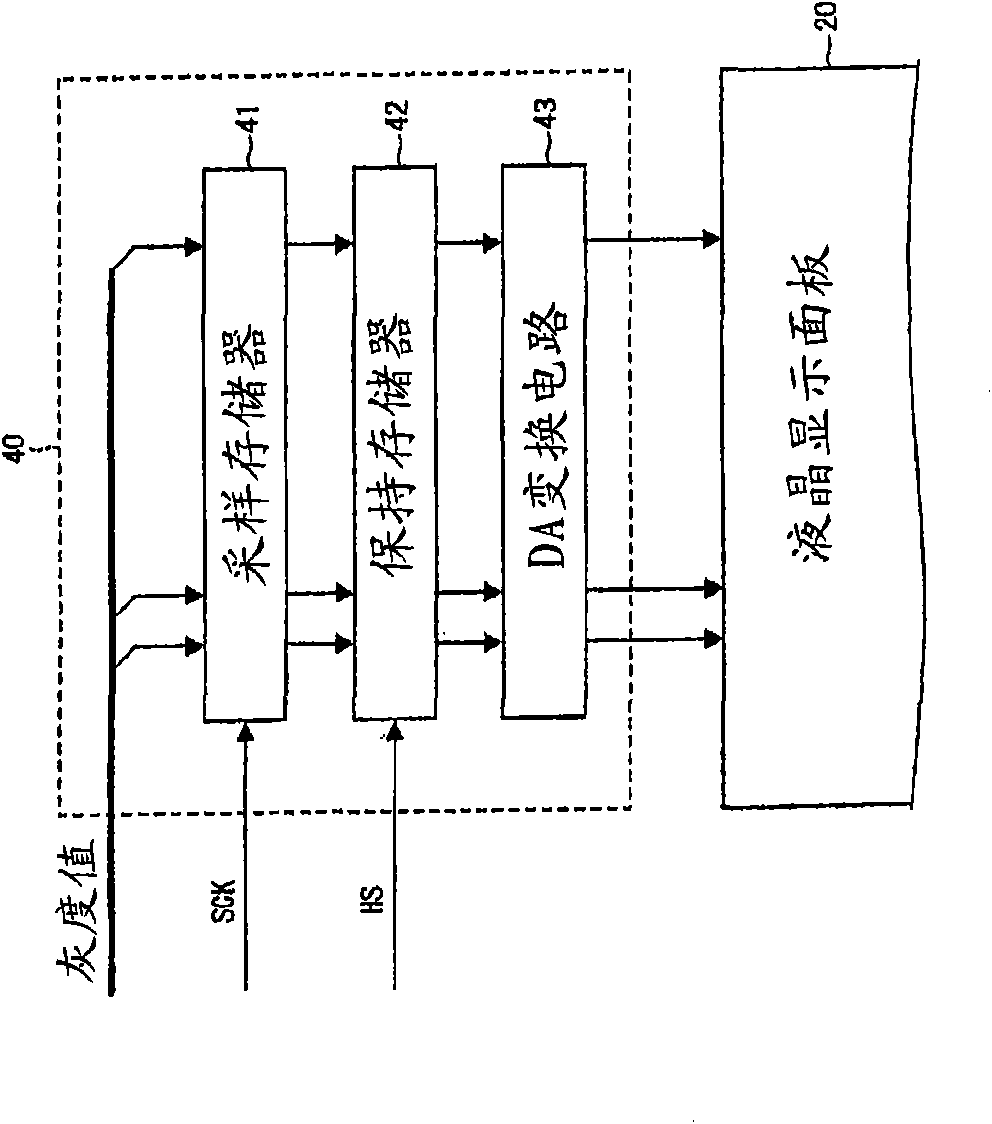
[0071] Such as figure 2 As shown, the liquid crystal display device 10 has a liquid crystal display panel 20 , a gate bus driving circuit 30 , a source bus driving circuit 40 and a control unit 50 .
[0072] Although not shown in particular, the liquid crystal display panel 20 is composed of a transparent substrate of a matrix substrate and an opposing substrate provided with opposing electrodes arranged in parallel with a predetermined interval therebetween, and liquid crystal is filled between th...
specific example 1
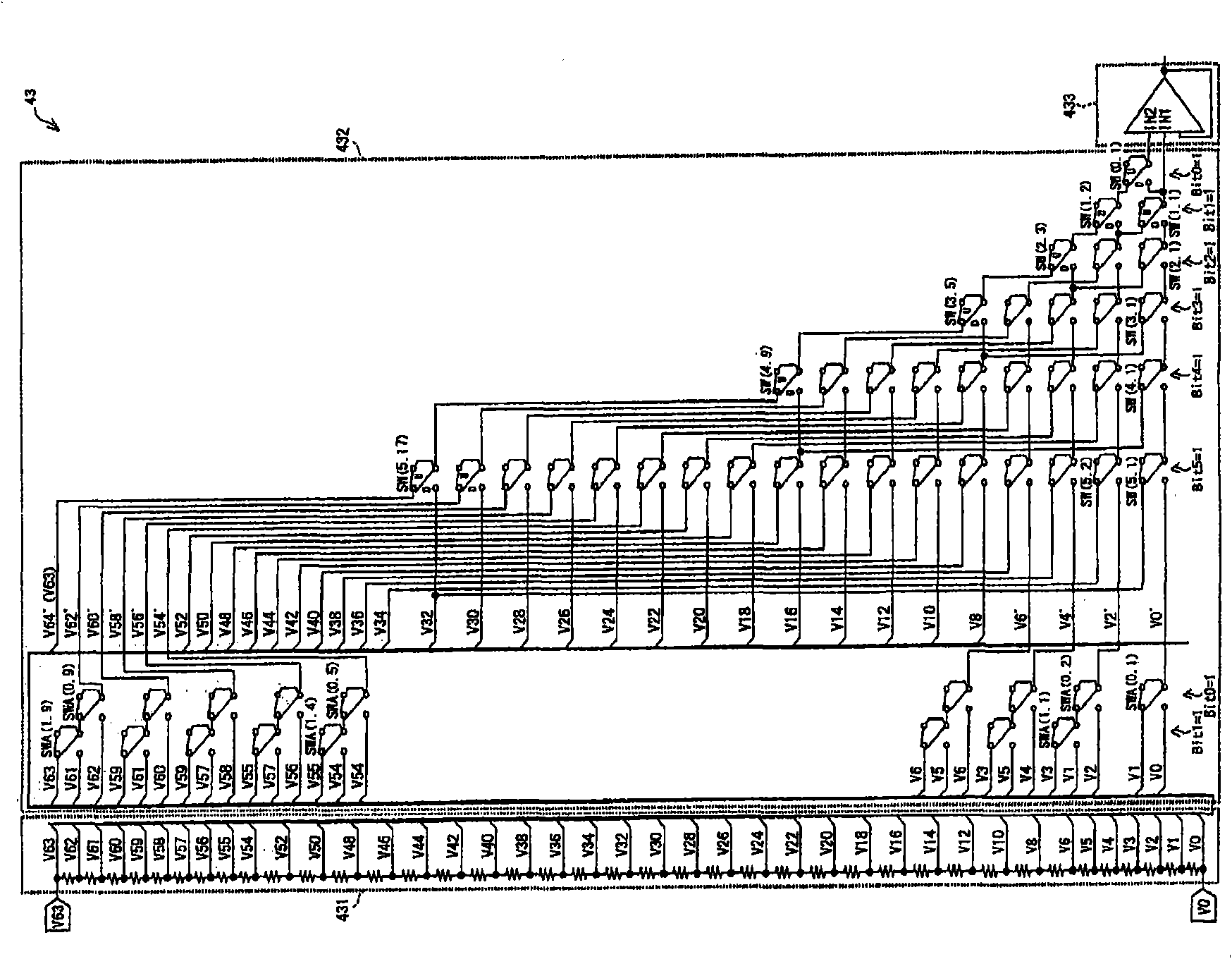
[0127] At once figure 1 In the example shown, the input bit string is the gray value "63" of "111111", all the switches on the upper side (in this figure) of the switch pair SW and SWA are turned on, and the switches on the lower side (in this figure) are turned on. All switches are non-conductive. As a result, the selection circuit 432 outputs the same voltage values as V to the input terminals IN1 and IN2 of the voltage follower circuit 433, respectively. 63 the reference voltage. The voltage follower circuit 433 will respond to the V input to the input terminal IN1 63 and input to the input terminal IN2 of V 63 The averaged voltage value is used as the gray voltage V OUT output, here, due to the input of the same voltage value V to both input terminals 63 , so the input V 63 as the grayscale voltage V OUT output.
specific example 2
[0129] Next, refer to Figure 4Next, the operation of the DA conversion circuit 43 when other gradation values are input from the control unit 50 will be described. Figure 4 It is an explanatory diagram for explaining the operation of the DA conversion circuit 43 when the input bit string is the grayscale value "5" of "000101".
[0130] Such as Figure 4 As shown, when the input bit string is the gray value "5" of "000101", in the selection circuit 432, the switch pair SW(0)U, SW(2)U and SWA(0)U are turned on, on the contrary, The switch pairs SW(0)D, SW(2)D and SWA(0)D are non-conductive. Furthermore, the switch pairs SW(5)U, SW(4)U, SW(3)U, SW(1)U and SWA(1)U are not conducting, on the contrary, the switch pairs SW(5)D, SW(4) )D, SW(3)D, SW(1)D and SWA(1)D are turned on. Thus, the selection circuit 432 inputs the same voltage value as V to the input terminals IN1 and IN2 of the voltage follower circuit 433, respectively. 5 the reference voltage. The voltage follower...
PUM
 Abstract
Description
Claims
Application Information


