Ball-planting device of semiconductor packaging equipment

A technology for packaging equipment and semiconductors, which is used in semiconductor/solid-state device manufacturing, electrical components, circuits, etc. It can solve the problems of high quality requirements for stencil hardware, low ball-mounting efficiency, and complex action mechanisms, and achieve control and debugging. Simple, less damage to solder balls, and the effect of reducing workload

Active Publication Date: 2011-02-09
厦门市原子通电子科技有限公司
View PDF0 Cites 5 Cited by
  • Summary
  • Abstract
  • Description
  • Claims
  • Application Information

AI Technical Summary

Problems solved by technology

This method has a complex action mechanism, requires image recognition systems, precise positioning systems, high-performance detection systems, and high-quality hardware such as stencils, and the price is extremely expensive.
The mechanism of the ball screening method is simple, but the ball planting accuracy is not high, the ball planting efficiency is not high, and it is easy to oxidize

Method used


Image

  • Ball-planting device of semiconductor packaging equipment
  • Ball-planting device of semiconductor packaging equipment
  • Ball-planting device of semiconductor packaging equipment

Examples


Embodiment Construction

[0019] The present invention will be further described below in conjunction with accompanying drawing.

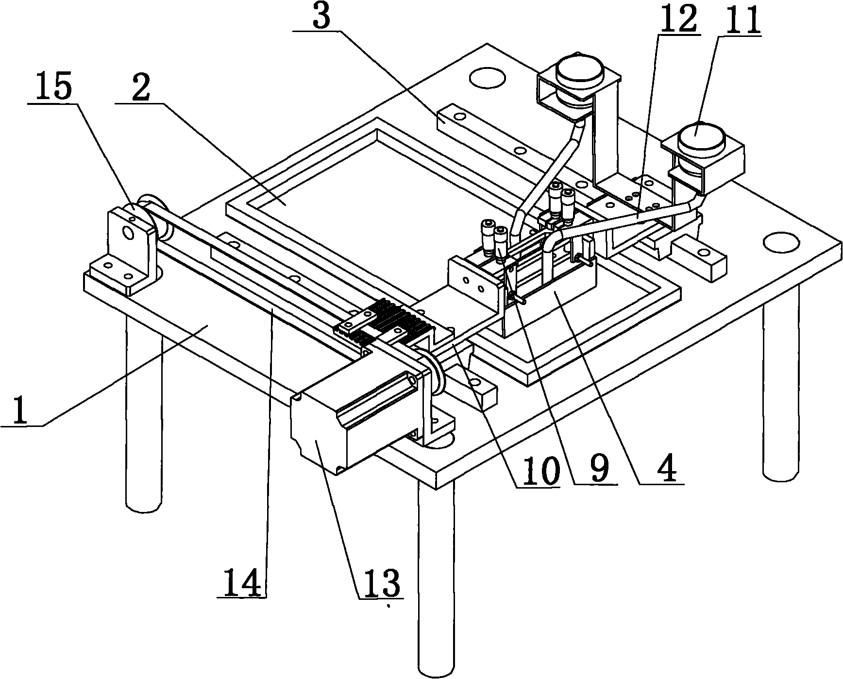
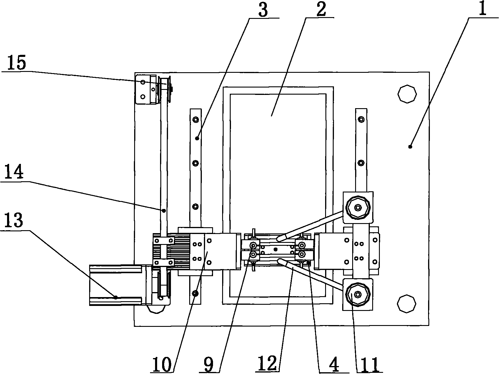
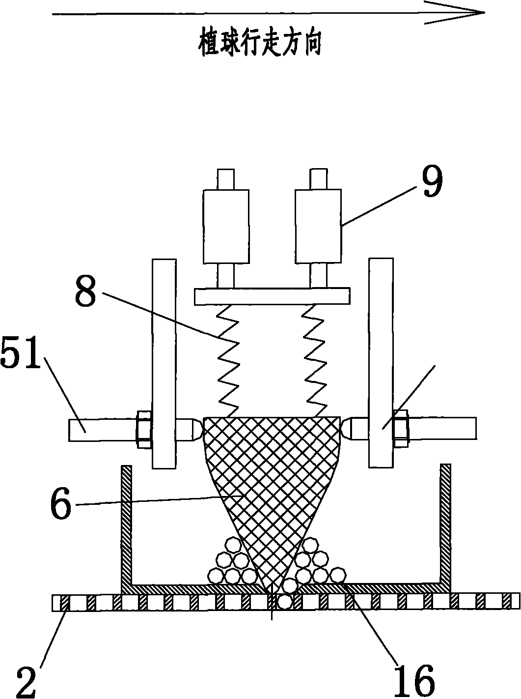
[0020] Such as figure 1 , 2 As shown, a ball planting device for semiconductor packaging equipment includes a frame 1, a screen 2, two guide rails 3, a ball planting mechanism and a drive mechanism, the screen 2 is fixed on the frame 1, and the The two guide rails 3 are respectively arranged on both sides of the screen plate 2, and the ball planting mechanism is located above the screen plate and is slidably fixed with the two guide rails 3. The ball planting mechanism includes a solder ball container 4 and a pair of stoppers 5. A scraper 6, a connecting plate 7, a plurality of springs 8, a plurality of dial gauges 9 and sensors, the solder ball container 4 is arranged on the screen 2, and the bottom of the solder ball container 4 is provided with a groove 40 , the pair of stoppers 5 are fixed on the solder ball container 4, the longitudinal section of the scraper 6 is ge...


PUM


Abstract

The invention relates to a ball-planting device of semiconductor packaging equipment, which comprises a stander, a net plate, two guide rails, a ball-planting mechanism and a driving mechanism. The net plate is fixed on the stander; the ball planting mechanism is positioned above the net plate and fixed in sliding fit with the two guide rails, and the ball-planting mechanism comprises a tin ball container, a pair of limit pieces, a scraper, a connecting plate, a plurality of springs, a plurality of dial indicators and a sensor; wherein the bottom of the tin ball container is provided with gaps, the pair of limit pieces is fixed on the tin ball container, the longitudinal section of the scraper has a cone shape with wide upside and narrow underside, the lower ends of the plurality of springs are fixed to the upper end of the scraper, the upper ends of the springs are connected with the plurality of dial indicators through the connecting plate, and the sensor is arranged in the tin ballcontainer; and the driving mechanism is in transmission connection with the ball-planting mechanism. The ball-planting device of the semiconductor packaging equipment has the advantages of low cost, simple and convenient control and debugging, wide applicability, little damage to tin balls, high success rate, high utilization rate, and the like.

Description

technical field [0001] The invention relates to an auxiliary device for semiconductor packaging, in particular to a ball planting device for semiconductor packaging equipment. Background technique [0002] In order to accurately implant solder balls into the substrate, the existing ball planting equipment basically adopts methods of ball sweeping, jig suction ball planting and ball screening. Sweeping the ball is to use a silk brush to make a rotating head to sweep the ball back and forth on the stencil to sweep the ball into the hole of the stencil and plant it on the substrate. This method has a complicated action mechanism, consumes a lot of silk brush, and the production process is cumbersome. , requires frequent replacement by professionals, and the cost is high; solder balls are wasteful in the process of sweeping the balls. The jig suction ball is to make a jig that is the same as the substrate, use the vacuum to suck the solder balls to the jig in the vibrating jig ...

Claims


Application Information

Patent Timeline
Patent Type & Authority Patents(China)
IPC IPC(8): H01L21/00H01L21/60
Inventor 徐光宇
Owner 厦门市原子通电子科技有限公司
Why Eureka
Try Eureka