
Method for switching main power supply and backup power supply and switching circuit

A backup power supply and switching circuit technology, applied in the direction of circuit devices, logic circuit coupling/interface using field effect transistors, emergency power supply arrangement, etc., can solve the problem that the switch switching control circuit output may not be correct, etc., to improve system reliability, The effect of avoiding substrate leakage and reducing requirements

Inactive Publication Date: 2009-12-16
HI TREND TECH SHANGHAI
View PDF1 Cites 31 Cited by
  • Summary
  • Abstract
  • Description
  • Claims
  • Application Information

AI Technical Summary

Problems solved by technology

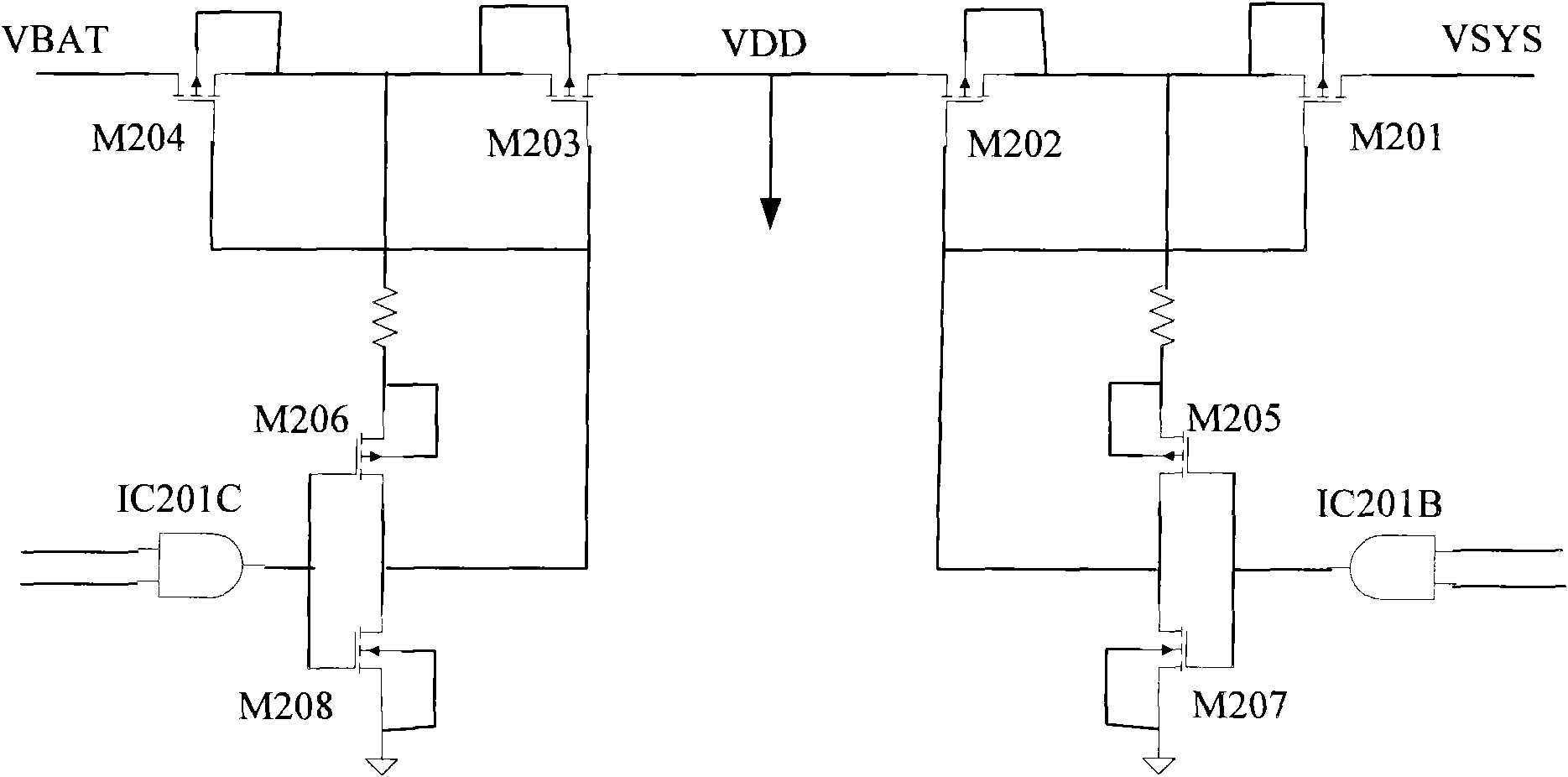
However, the shortcoming of this patent is that M201, M202, M203 and M204 series switches must be turned on and off at the same time, otherwise leakage through the parasitic diode of the PMOS substrate may occur. For example, when VDD=VBAT, if the switch M202 is turned off, but the switch M201 is turned on, Then when VDD>VSYS, VDD will leak to VSYS through the substrate diode of the switch M202, and in some specific applications, such a control logic that is not on and off at the same time may be required; second, when VDD is too low, the switch switches The output of the control circuit may not be correct, that is to say, even if VSYS recovers at this time, the control circuit may not be able to give correct information, switch the switch to use VSYS for power supply

Method used


Image

  • Method for switching main power supply and backup power supply and switching circuit
  • Method for switching main power supply and backup power supply and switching circuit
  • Method for switching main power supply and backup power supply and switching circuit

Examples


Embodiment Construction

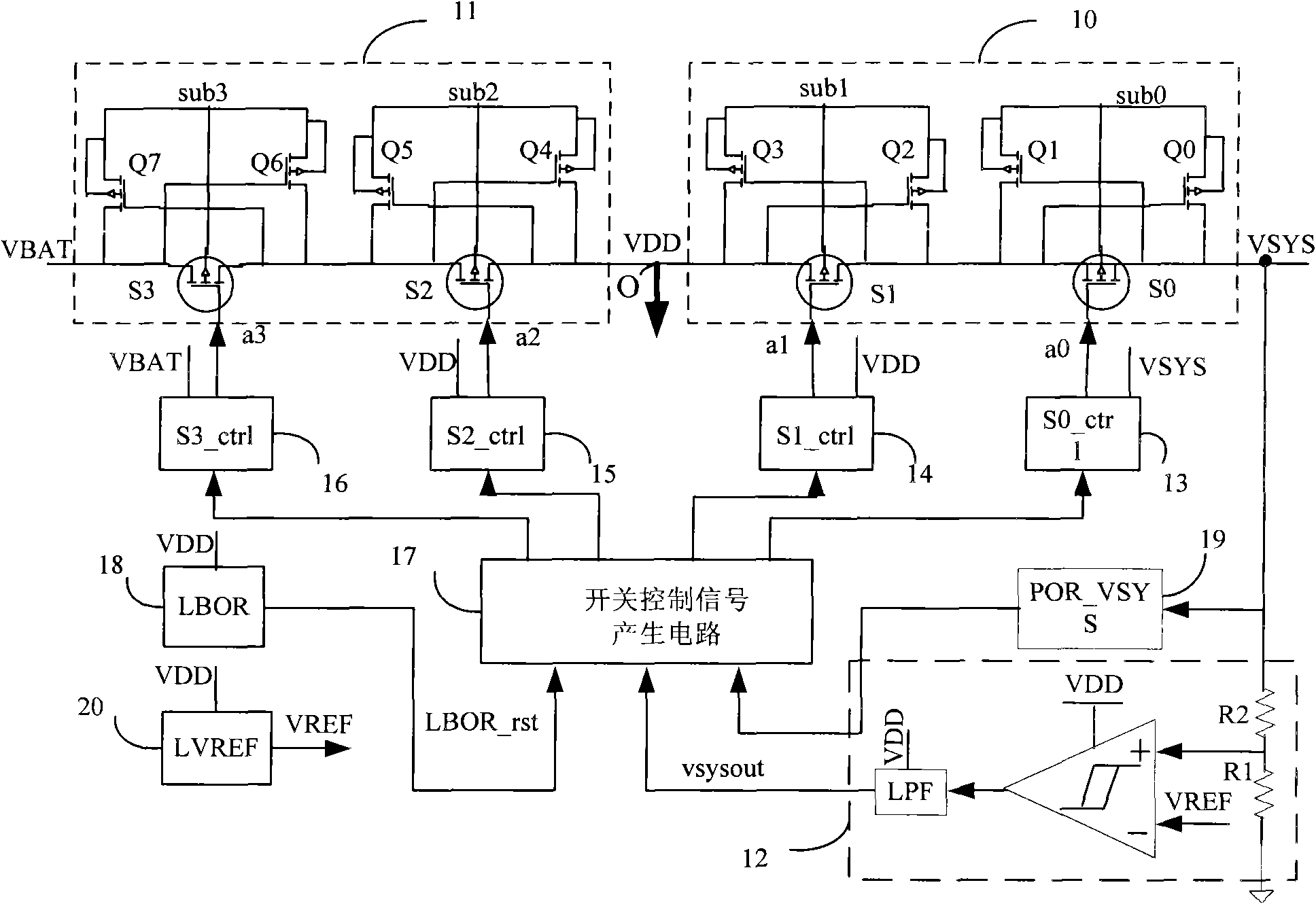
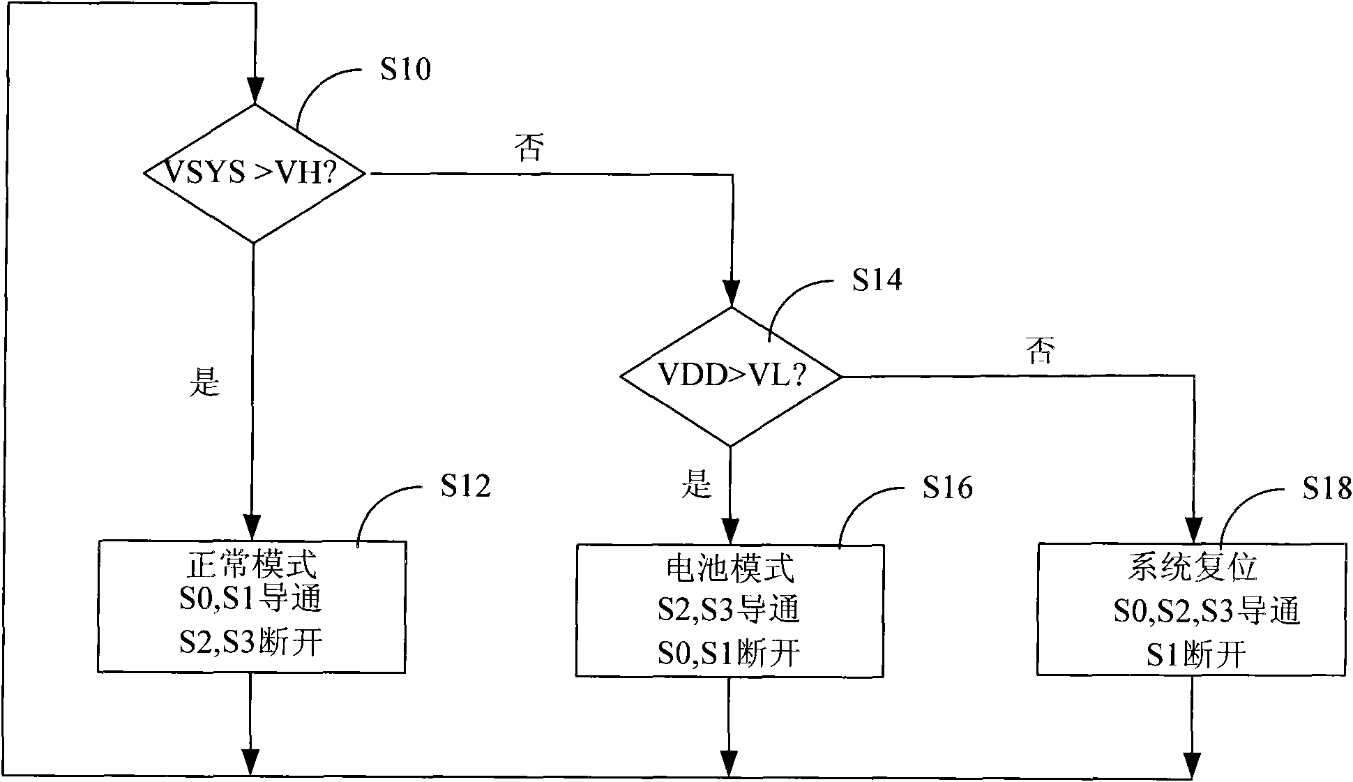
[0024] figure 2 A schematic diagram of a switching circuit according to an embodiment of the present invention is shown. refer to figure 2 As shown, this switching circuit includes a power supply double switch, a detection part and a switch switching control part. Specifically, the dual power switch includes a main power switch 10 and a backup power switch 11. The main power switch 10 is composed of a first PMOS transistor S0 and a second PMOS transistor S1 connected in series to provide electrical conduction between the main power supply VSYS and the output node O. Path: The backup power switch 11 is composed of a third PMOS transistor S2 and a fourth PMOS transistor S3 connected in series to provide a conductive path between the backup power supply (such as a battery) VBAT and the output node O. The output node O is used to output the voltage VDD, which can be used as an uninterrupted internal power supply voltage for various electric circuits.

[0025] In one embodimen...


PUM


Abstract

The invention discloses a method for switching a main power supply and a backup power supply and a switching circuit. The switching circuit comprises a main power supply switch, a backup power supply switch, a first switch control logic to a fourth switch control logic, a main power supply detection circuit and a switch control signal generation circuit, wherein, the main power supply switch comprises a first PMOS pipe and a second PMOS pipe; the first PMOS pipe and the second PMOS pipe are connected in series between the main power supply and an output node; the backup power supply switch comprises a third PMOS pipe and a fourth PMOS pipe; the third PMOS pipe and the fourth PMOS pipe are connected in series between the output node and the backup power supply; and the switch control signal generation circuit determines connection and stop of the first PMOS pipe to the fourth PMOS pipe according to input of the main power supply detection circuit. Independent substrates of the PMOS pipes are generated through a mode of cross coupling, which not only can avoid substrate creepage, but also can meet the requirement of respectively connecting and stopping two serially connected PMOS pipes.

Description

technical field [0001] The invention relates to a dual power supply system with a backup power supply, in particular to a dual power supply system capable of seamlessly switching between the main power supply and the backup power supply by controlling a MOS switch when the main power supply drops or recovers. Background technique [0002] With the development of science and technology, more and more equipment and precision instruments, such as communication terminal equipment, bank computer systems, surgical equipment and many high-precision instruments for measurement, need an uninterrupted and stable working power supply. Based on this These devices and instruments often have two or more power supplies to power them, one of which is the main power supply, and the rest are secondary power supplies. When the system works normally, the internal voltage of the system is usually provided by the main power supply, and the auxiliary power supply is disconnected from the system; w...

Claims


Application Information

Patent Timeline
Patent Type & Authority Applications(China)
IPC IPC(8): H02J9/06H03K19/0185H03K17/687
Inventor 姚超朱江
Owner HI TREND TECH SHANGHAI
Learn More