Mass production method for ultra-fine bonding gold wire

A production method and alloy wire technology, applied in furnaces, heat treatment equipment, manufacturing tools, etc., can solve problems such as difficulty in production, alarm, and low yield.

Inactive Publication Date: 2009-12-23
北京达博有色金属焊料有限责任公司
View PDF2 Cites 19 Cited by
  • Summary
  • Abstract
  • Description
  • Claims
  • Application Information

AI Technical Summary

Problems solved by technology

[0005] However, the thinner the gold wire, the more difficult it is to produce, the more difficult it is to draw the wire, and it is very easy to break or the gold wires will stick to each other, resulting in a low yield, especially for ultra-fine bonding gold wires of 17 microns and below. In production, it is particularly obvious that the existing improvement methods generally only improve the composition of raw materials, such as "A Bonding Gold Wire and Its Manufacturing Method" in Chinese Patent 200610021373.2, and some improve the production method, such as in Chinese Patent 200410017008.5 "Preparation method of ultra-fine wire of non-ferrous metal and its alloy material", which uses the horizontal directional continuous casting process to improve the performance of the cast billet to increase the yield. At present, these existing gold wire production methods can basically meet the requirements of 18 microns and above. The mass production of alloy wire is required, and the ultra-fine bonding gold wire of 17 microns and below is produced through the existing production process, which frequently breaks the wire during the processing process and the production efficiency is low. At the same time, customers are prone to quality problems when using such gold wire. For example, the surface quality of the gold wire is not good, the wire is not good, the performance is unstable, etc., the gold wire is prone to sticking, wire breakage or equipment alarm during bonding, resulting in low bonding efficiency and yield, and cannot effectively meet customer needs.

Method used


Image

  • Mass production method for ultra-fine bonding gold wire
  • Mass production method for ultra-fine bonding gold wire

Examples


Embodiment Construction

[0022] In order to allow the above-mentioned and other objects, features and advantages of the present invention to be more clearly understood, the preferred embodiments of the present invention are now specifically cited, together with the accompanying drawings, as follows in detail:

[0023] The large-scale production method of ultra-fine bonding gold wire of the present invention is an improvement of the existing production process, so the common points with the prior art will not be described in detail, and the improved process of the present invention will be described in detail here.

[0024] Common bonded gold wire production methods include casting process (alloy casting), wire drawing process (large drawing, medium drawing, fine drawing, ultra-fine drawing), annealing process (finished product annealing, performance testing), winding process (size Rewind).

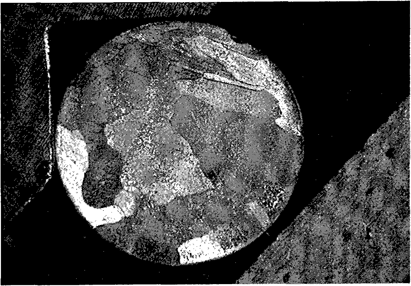
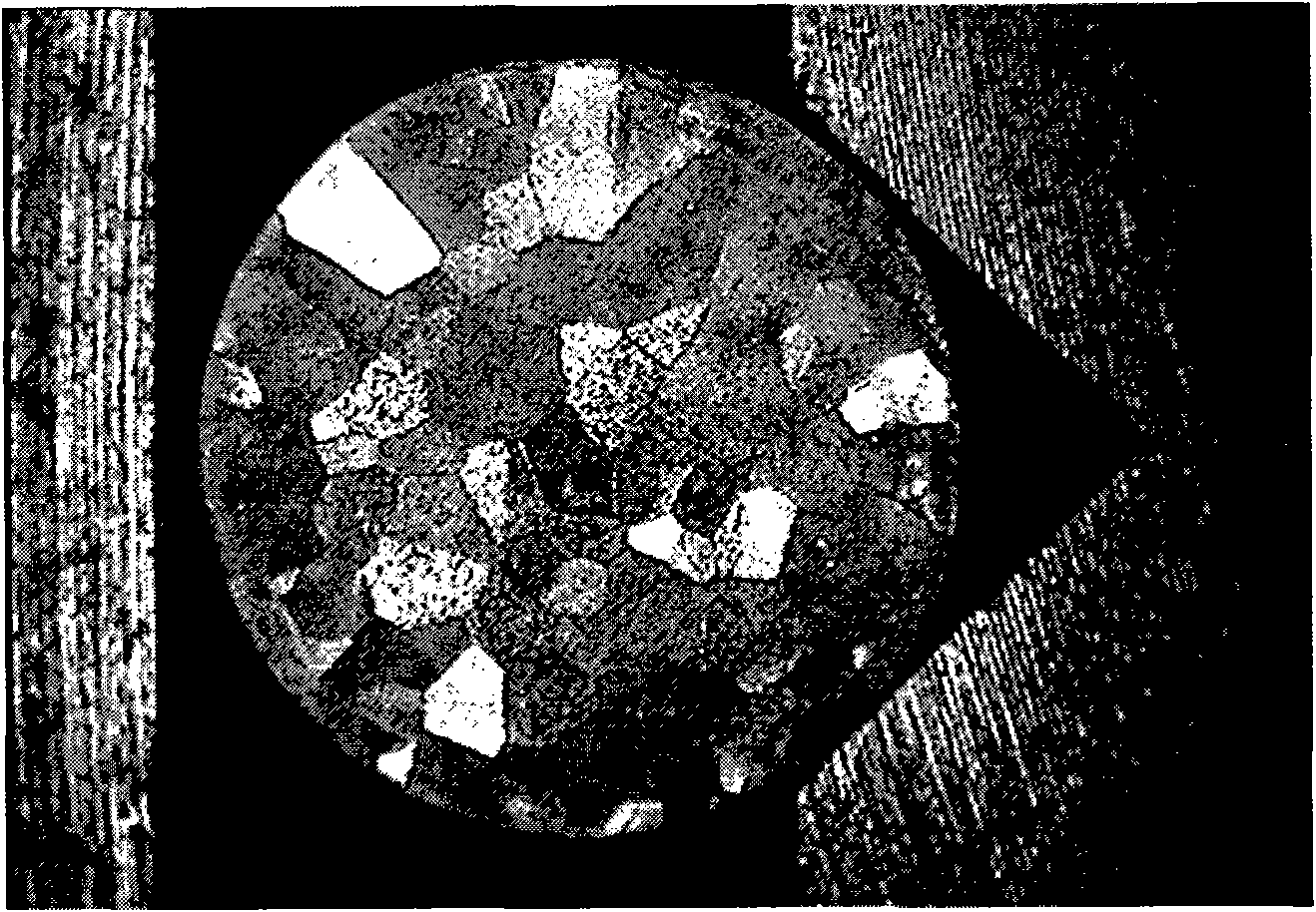
[0025] Among them, the melting and casting alloying process is the basis, which determines the processability a...


PUM

PropertyMeasurementUnit
lengthaaaaaaaaaa
lengthaaaaaaaaaa

Abstract

The invention discloses a mass production method for an ultra-fine bonding gold wire. The production method comprises the steps of a fusion casting process (alloy fusion casting), a fiber drawing process (coarse drawing, intermediate drawing, fine drawing and ultrafine drawing), an annealing process (final annealing and performance test), a winding process (fixed size compound winding) and the like. The method improves the alloy fusion casting process and the annealing process aiming at the mass production of the ultra-fine bonding gold wire, in the fusion casting process, by mainly utilizing the intermittent pull casting, and intermittently inhibiting the formation of columnar crystal, the small shaft diameter is formed conveniently, so that the extensibility of a cast ingot is ensured, and simultaneously certain strength can also be achieved, and the processing requirements of the ultra-fine bonding gold wire are better met. The product prepared by the method is suitable for the miniaturization packaging requirements of integrated circuits and large scale integrated circuits as well as low-cost requirements of packaging discrete devices and LEDs. The method has the characteristics of high yield of the ultrafine wire and good consistency among batch materials, and meets the requirements of batch and mass stable production.

Description

technical field [0001] The invention relates to a production method of bonding gold wire, in particular to a method for large-scale production of ultrafine bonding gold wire. Background technique [0002] With the rapid development of the microelectronics industry, the microelectronics process continues to improve, the IC characteristic parameters continue to shrink, and the integration level increases at an alarming rate. Since the VLSI integration level has been following the "Moore's Law" to double every 18 months, it has increased sharply. At present, the number of circuit elements integrated on a chip has already exceeded 100 million, so this development trend is changing the role of VLSI in electronic equipment from device chips to system chips (SOC); at the same time, deep submicron VLSI The feature size of the process has reached below 0.18μm. In the case of continuous shrinking of feature size, increasing integration, chip area, and actual power consumption, the pro...

Claims


Application Information

Patent Timeline
Patent Type & Authority Applications(China)
IPC IPC(8): B23P17/00B22D11/00B22D11/16B22D11/112C22B9/04C21D9/52
CPCH01L24/43H01L2224/43848H01L2224/45144H01L2924/14H01L2224/45H01L2224/43H01L2924/00H01L2924/00012
Inventor 刘家强杨顺兴苏宏福杜连民向翠华
Owner 北京达博有色金属焊料有限责任公司
Why Eureka
Try Eureka