Maintenance control method and system used for semiconductor processing equipment

A technology for processing equipment and maintenance control, applied in the field of microelectronics, can solve the problems of waste of human, financial and material resources, small coupling of functional modules, and reduced production efficiency of semiconductor factories, so as to achieve high production efficiency and avoid waste.

Active Publication Date: 2011-07-27
BEIJING NAURA MICROELECTRONICS EQUIP CO LTD
View PDF0 Cites 0 Cited by
  • Summary
  • Abstract
  • Description
  • Claims
  • Application Information

AI Technical Summary

Problems solved by technology

Although this maintenance control method can realize the maintenance of the semiconductor processing equipment, in practical applications, this maintenance method has a strong dependence on historical data, that is to say, the maintenance control method is based on historical data. Judging whether the current semiconductor processing equipment needs maintenance, rather than making judgments and maintenance based on the actual status of the current semiconductor processing equipment
Therefore, such a maintenance method has the following problems: it not only wastes human, material and financial resources, but also reduces the production efficiency of the semiconductor factory
[0010] Although prior art 2 can determine whether the functional modules need to be maintained according to the current working conditions of the functional modules inside the semiconductor processing equipment, in practical applications, because each functional module in the semiconductor processing equipment usually adopts distributed control Therefore, the coupling between each functional module is small. In this case, if a certain functional module needs maintenance, regardless of whether it is a parallel module or a serial module, the entire semiconductor processing equipment will be stopped before the next process task. Switching to maintenance operations will not only cause waste of human, financial and material resources, but also reduce the production efficiency of the entire semiconductor processing equipment

Method used


Image

  • Maintenance control method and system used for semiconductor processing equipment
  • Maintenance control method and system used for semiconductor processing equipment
  • Maintenance control method and system used for semiconductor processing equipment

Examples


Embodiment Construction

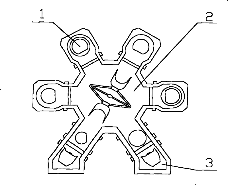
[0040] In order to enable those skilled in the art to better understand the technical solution of the present invention, the following in conjunction with the accompanying drawings and figure 1 The semiconductor processing equipment shown is taken as an example, and the maintenance control method and system for semiconductor processing equipment provided by the present invention and the semiconductor processing equipment provided by the present invention are described in detail. The semiconductor processing equipment includes functional modules such as a wafer aligner, a vacuum manipulator, an atmospheric manipulator, a vacuum lock chamber, a transfer chamber, and multiple reaction chambers. Wherein, two vacuum lock chambers can be called a group of parallel modules, and multiple reaction chambers can also be called a group of parallel modules.

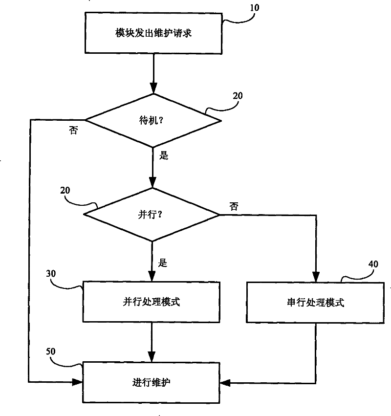
[0041] see figure 2 , the maintenance control method provided by the present invention may include the following steps:

[0042] ...


PUM


Abstract

The invention discloses a maintenance control used for semiconductor processing equipment. The method comprises the following steps of: judging a function module sending a maintaining request; processing the maintaining request by a parallel processing mode, if the function module is a parallel module and not in a standby state; processing the maintaining request by a serial processing mode, if the function module is a serial module and not in the standby state; and directly maintaining the function module needing maintaining, if the function module is in the standby state. In addition, the invention also provides a maintenance control system used for the semiconductor processing equipment and the semiconductor processing equipment. The maintenance control method and the maintenance control system can effectively maintain the semiconductor processing equipment in time, and also can keep higher production efficiency and reduce / avoid waste. The semiconductor processing equipment not only can be effectively maintained in time, but also can keep higher production efficiency and reduce / avoid the waste when maintained.

Description

technical field [0001] The invention relates to the technical field of microelectronics, in particular to a maintenance control method and system for semiconductor processing equipment. Furthermore, the present invention also relates to a semiconductor processing device. Background technique [0002] With the rapid development of electronic technology, people have higher and higher requirements for the integration of integrated circuits, which requires companies that produce integrated circuits to continuously improve the processing / processing capabilities of semiconductor devices. Currently, plasma processing techniques such as plasma deposition techniques, plasma etching techniques, and the like are widely used in the processing / processing of semiconductor devices. These plasma processing technologies usually need to be realized by means of corresponding semiconductor processing equipment. [0003] see figure 1 , the existing semiconductor processing equipment usually i...

Claims


Application Information

Patent Timeline
Patent Type & Authority Patents(China)
IPC IPC(8): G05B19/418H01L21/00
CPCY02P90/02Y02P90/80
Inventor 崔琳
Owner BEIJING NAURA MICROELECTRONICS EQUIP CO LTD
Why Eureka
Try Eureka