Circuit substrate and its formation method and semiconductor encapsulation

A circuit substrate and semiconductor technology, applied in semiconductor devices, semiconductor/solid-state device manufacturing, semiconductor/solid-state device components, etc., can solve problems such as difficult formation of multi-layer circuit lines

Inactive Publication Date: 2010-01-06
SK HYNIX INC
View PDF0 Cites 10 Cited by
  • Summary
  • Abstract
  • Description
  • Claims
  • Application Information

AI Technical Summary

Problems solved by technology

However, since the area of ​​wafer-level packaging is extremely small, it is difficult to form multilayer circuit lines

Method used


Image

  • Circuit substrate and its formation method and semiconductor encapsulation
  • Circuit substrate and its formation method and semiconductor encapsulation
  • Circuit substrate and its formation method and semiconductor encapsulation

Examples


Embodiment Construction

[0076] A circuit substrate, a method of manufacturing the circuit substrate, and a semiconductor package with circuit lines according to specific embodiments of the present invention will be described in detail below with reference to the accompanying drawings.

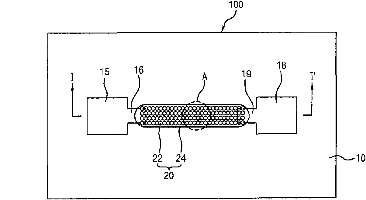
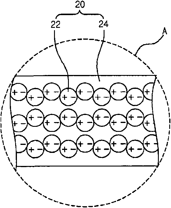
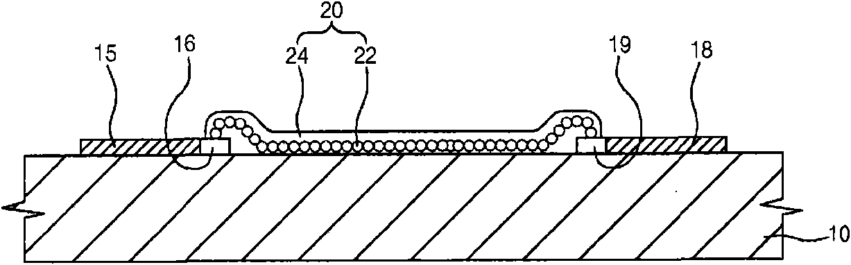
[0077] figure 1 A plan view of a circuit substrate according to a specific embodiment of the present invention is shown. figure 2 Yes figure 1 Partial enlarged view of part 'A' of . image 3 for along figure 1 The cross-sectional view of the I-I' line.

[0078] refer to figure 1 , the circuit substrate 100 includes a substrate main body 10 and circuit lines 20 .

[0079] The substrate main body 10 may be in the shape of a plate, or may be a printed circuit board. Alternatively, the substrate body 10 may have a different shape, and may be an insulating plate or a semiconductor chip.

[0080] The first terminal 15 and the second terminal 18 may be disposed on the upper surface of the substrate body 10 , the firs...


PUM


Abstract

The invention discloses a circuit substrate and its formation method and semiconductor encapsulation. The circuit substrate includes a substrate body having a first terminal and a second terminal separated from the first terminal. A circuit wire includes a wiring unit for electrically connecting the first and second terminals by electrically connecting conductive polarization particles that include a first polarity and a second polarity that is opposite to the first polarity. The circuit wire also includes an insulation unit for insulating the wiring unit.

Description

technical field [0001] The present invention relates to a circuit substrate with circuit lines, a method of manufacturing the circuit substrate, and a semiconductor package with the circuit lines, in particular to a circuit substrate with circuit lines formed of conductive polarized particles. Background technique [0002] Recently, various electronic devices and products utilizing technologies developed in the electronics industry have been developed. Most electronic devices and products contain circuit substrates for mounting electrical appliances, electronic devices, and semiconductor packages thereon. [0003] The circuit substrate includes circuit lines for electrically connecting electrical appliances, electronic devices, and semiconductor packages. [0004] It is known that circuit lines are formed by patterning a metal layer formed on an insulating substrate. However, when the circuits formed on the insulating substrate cross each other on the same surface, a short...

Claims


Application Information

Patent Timeline
Patent Type & Authority Applications(China)
IPC IPC(8): H01L23/488H01L23/498H01L21/48H01L23/485
CPCH01L2224/24998H01L2224/73204H01L2924/01082H01L2924/01013H01L2224/32225H01L24/19H01L2924/01029H01L2924/01047H01L2224/82007H01L2224/16225H01L2924/01006H01L2224/24145H01L2924/01033H01L24/24H01L2225/06562H01L2924/01079H01L2224/02315H01L2224/12105H01L2224/19H01L2224/24H01L2924/00H01L2924/00012H05K1/02
Inventor 姜泰敏
Owner SK HYNIX INC
Why Eureka
Try Eureka