Solid-state image pickup apparatus, method of manufacturing the same, and electronic apparatus

A camera device and camera pixel technology, which is applied in radiation control devices, televisions, circuits, etc., can solve the problems that camera pixels and focus detection pixels are not easy to form microlenses, and image quality is degraded, so as to optimize the separation characteristics and simplify the formation process. Effect

Active Publication Date: 2015-04-15
SONY CORP
View PDF6 Cites 9 Cited by
  • Summary
  • Abstract
  • Description
  • Claims
  • Application Information

AI Technical Summary

Problems solved by technology

[0006] However, in the structure disclosed in Japanese Patent Application Laid-Open No. 2009-109965, it is not easy to commonly form microlenses for imaging pixels and focus detection pixels
[0007] In addition, in the structure of Japanese Patent Application Laid-Open No. 2007-281296, in the focus detection pixel, since the microlens is higher than the imaging pixel, a shadow is generated in the imaging pixel adjacent to the focus detection pixel, thereby causing deterioration in image quality. deterioration

Method used


Image

  • Solid-state image pickup apparatus, method of manufacturing the same, and electronic apparatus
  • Solid-state image pickup apparatus, method of manufacturing the same, and electronic apparatus
  • Solid-state image pickup apparatus, method of manufacturing the same, and electronic apparatus

Examples


Embodiment Construction

[0039] Hereinafter, embodiments of the present invention will be described with reference to the drawings.

[0040] Structural example of a solid-state imaging device

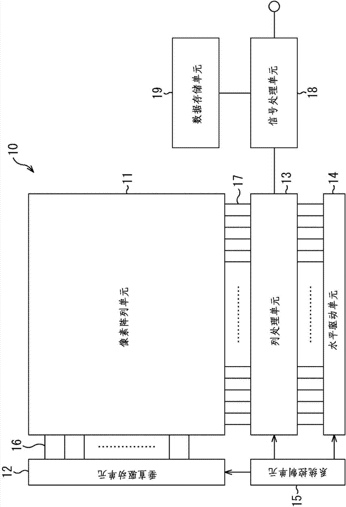
[0041] figure 1is a block diagram showing a configuration example of the solid-state imaging device of the present invention. Next, a description will be given of a rear surface illumination type complementary metal oxide semiconductor (CMOS) image sensor (an amplifying type solid-state imaging device). It should be noted that the present invention is applicable not only to rear-surface-illuminated CMOS image sensors, but also to other amplification-type solid-state imaging devices such as front-surface-illuminated CMOS image sensors or image sensors such as charge-coupled devices (CCDs). A class of charge transport type solid-state imaging devices.

[0042] figure 1 The illustrated CMOS image sensor 10 includes a pixel array unit 11 formed on a semiconductor substrate (not shown) and a peripheral circuit u...


PUM


Abstract

A solid-state image pickup apparatus includes an image pickup pixel and a focus detection pixel. The image pickup pixel includes a micro lens and a photoelectric conversion unit that receives light incident from the micro lens. The focus detection pixel includes the micro lens, the photoelectric conversion unit, and a light shielding unit that shields part of light incident on the photoelectric conversion unit. In the solid-state image pickup apparatus, the micro lens is uniformly formed in the image pickup pixel and the focus detection pixel, and the focus detection pixel further includes a high refractive index film formed under the micro lens.

Description

technical field [0001] The present invention relates to a solid-state imaging device, a manufacturing method of the solid-state imaging device, and electronic equipment, and particularly to a solid-state imaging device capable of optimizing the sensitivity of imaging pixels and the separation characteristics of focus detection pixels, a manufacturing method of the solid-state imaging device, and Electronic equipment. Background technique [0002] A conventionally known solid-state imaging device performs focus detection by a so-called pupil division phase difference system that detects a focus point based on shift amounts of signals output from pairs of focus detection pixels. In a solid-state imaging device, focus detection pixels are provided to a pixel array unit having imaging pixels. [0003] In such a solid-state imaging device, the imaging pixel exhibits the highest sensitivity in the case where there is a light-collecting point of a microlens on the light-receiving ...

Claims


Application Information

Patent Timeline
Patent Type & Authority Applications(China)
IPC IPC(8): H01L27/146H01L27/148H04N5/335
CPCH01L27/14625H01L27/14685H01L27/14627H01L27/14645H04N5/23212H04N5/369
Inventor 冈治
Owner SONY CORP
Why Eureka
Try Eureka