Formation method for VDMOS (vertical double-diffused metal oxide semiconductor) device

A device and epitaxial layer technology, which is applied in the field of VDMOS device formation, can solve the problems of affecting the isolation effect, damaging the insulating performance of the second gate oxide layer, and being difficult to chemical mechanical polishing, and achieves the effect of improving electrical performance.

Active Publication Date: 2011-08-10
SHANGHAI HUAHONG GRACE SEMICON MFG CORP
View PDF3 Cites 9 Cited by
  • Summary
  • Abstract
  • Description
  • Claims
  • Application Information

AI Technical Summary

Problems solved by technology

Because the first gate oxide layer 50 is located in the recessed opening, it is not easy to perform chemical mechanical polishing
[0014] Further, if the thickness of the first gate oxide layer 50 is small, it may be lower than the isolation structure between VDMOS devices, and the grinding process will cause damage to the isolation structure, affecting the isolation effect
[0015] Fu

Method used


Image

  • Formation method for VDMOS (vertical double-diffused metal oxide semiconductor) device
  • Formation method for VDMOS (vertical double-diffused metal oxide semiconductor) device
  • Formation method for VDMOS (vertical double-diffused metal oxide semiconductor) device

Examples


Embodiment Construction

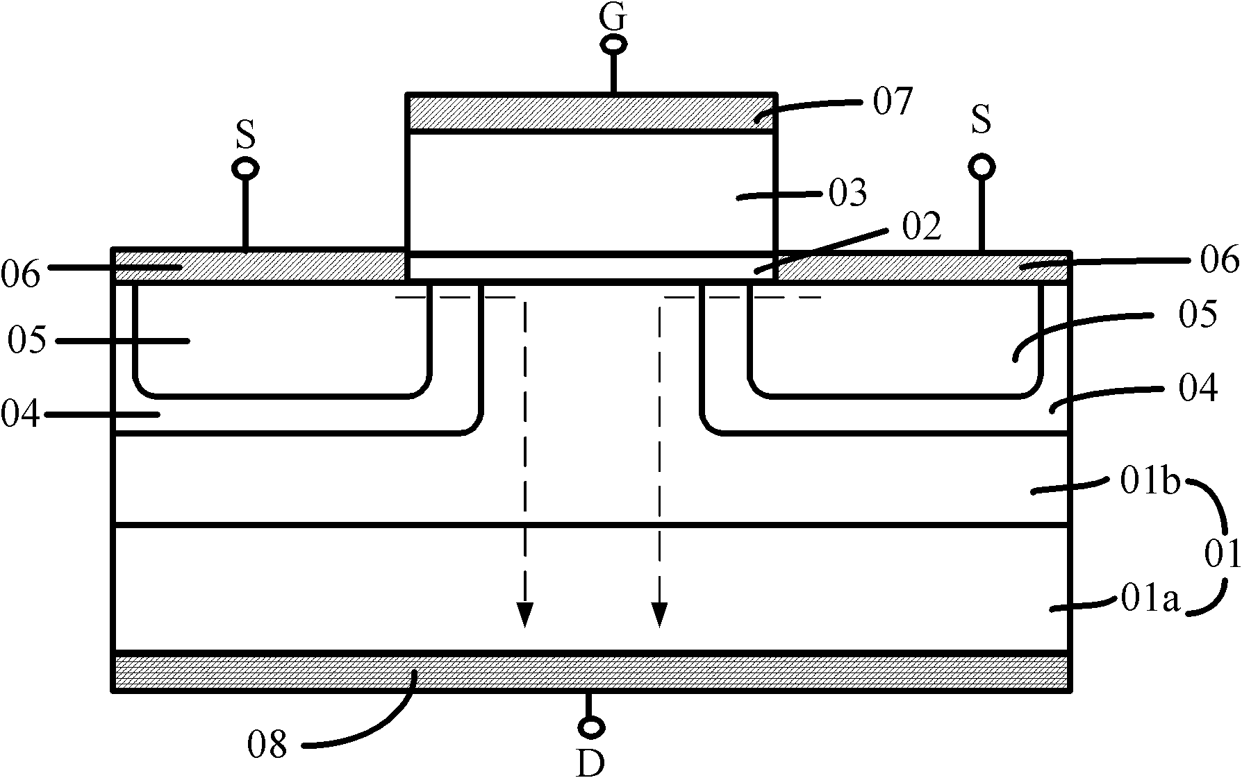
[0044] Such as Figure 7 As shown, the existing technology increases the thickness of the gate oxide layer between the drain D and the gate G by adding a second gate oxide layer 50 between the drain D and the gate G, and reduces the gap between the gate and the drain. The capacitor value increases the switching speed of VDMOS. However, the second gate oxide layer 50 is formed by deposition and chemical mechanical polishing, that is, the filled oxide needs to be chemical mechanical polishing to reach a predetermined thickness. Because the second gate oxide layer 50 is located in the recessed opening, it is not easy to perform chemical mechanical polishing.

[0045]In order to solve the above problems, the present invention provides a method for forming a VDMOS device, comprising: providing a semiconductor substrate on which an epitaxial layer is formed; forming a sacrificial layer with an opening on the surface of the epitaxial layer, and the opening Exposing the surface of t...


PUM

PropertyMeasurementUnit
Thicknessaaaaaaaaaa
Thicknessaaaaaaaaaa

Abstract

The invention provides a formation method for a VDMOS (vertical double-diffused metal oxide semiconductor) device, which comprises the following steps: providing a semiconductor substrate and forming an epitaxial layer on the semiconductor substrate; forming a sacrificial layer with an opening on the surface of the epitaxial layer, wherein the opening is exposed out of the surface of the epitaxial layer; thermally oxidizing the epitaxial layer in the opening so as to form a first grid electrode oxidation layer; removing the sacrificial layer; thermally oxidizing the epitaxial layer so as to form a second oxidation layer; depositing a polycrystalline silicon layer which covers the first grid electrode oxidation layer and the second oxidation layer; etching the polycrstaslline silicon layer and the second oxidation layer so as to form a grid electrode structure; and forming a source region, a source electrode metal layer, a drain electrode metal layer and a grid electrode metal layer. The formation method reduces the technology difficulty of the grid electrode oxidation layer and increases the thickness of the grid electrode oxidation layer between a drain electrode and a grid electrode, so as to reduce the capacitance value between the grid electrode and the drain electrode and increase the switching speed of the VDMOS.

Description

technical field [0001] The invention relates to a power device, in particular to a method for forming a VDMOS device. Background technique [0002] Vertical double diffused metal oxide semiconductor field effect transistor (VDMOS), as a kind of power device, is widely used because of its advantages of high input impedance and low conduction voltage drop. The formation method of the prior art VDMOS device is as disclosed in the Chinese patent application whose publication number is CN 101515547A, specifically as figure 1 Shown is a schematic structural view of VDMOS, including: a semiconductor substrate 01, the semiconductor substrate 01 includes a semiconductor substrate 01a and an epitaxial layer 01b located on the semiconductor substrate 01a; a gate structure located on the surface of the epitaxial layer 01b, the The gate structure includes a gate oxide layer 02, a gate polysilicon layer 03 and a gate metal layer 07 sequentially located on the surface of the gate oxide la...

Claims


Application Information

Patent Timeline
IPC IPC(8): H01L21/336H01L21/28
Inventor 楼颖颖克里丝
Owner SHANGHAI HUAHONG GRACE SEMICON MFG CORP
Why Eureka
Try Eureka