LED electrode structure

An electrode structure and electrode technology, applied in the direction of circuits, electrical components, semiconductor devices, etc., can solve problems such as uneven luminous brightness, low conductivity, and uneven current distribution

Inactive Publication Date: 2010-01-20
SUN YAT SEN UNIV
View PDF0 Cites 5 Cited by
  • Summary
  • Abstract
  • Description
  • Claims
  • Application Information

AI Technical Summary

Problems solved by technology

For traditional nitride light-emitting diodes, due to the low conductivity of P-type nitride, the lateral conductivity of the current in it is much lower than the vertical conductivity, so that the current cannot be effectively and evenly distributed after being injected from the contact part. The light-emitting layer of the light-emitting diode can only be distributed in the effective area of ​​the P-type nitride semiconductor layer under the P-type contact electrode, and cannot be distributed laterally to the entire P-type nit

Method used


Image

  • LED electrode structure
  • LED electrode structure
  • LED electrode structure

Examples


Embodiment 1

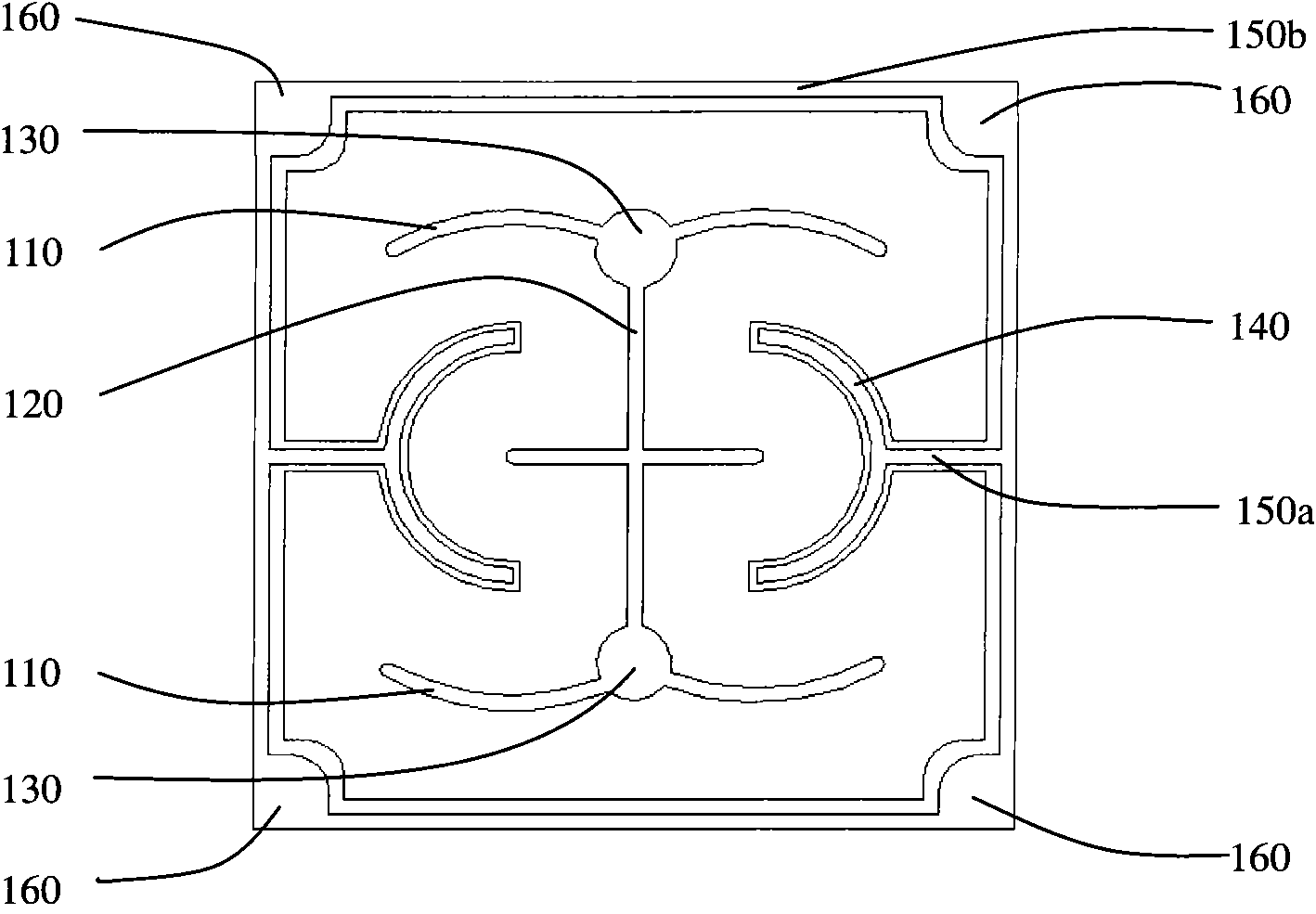
[0037] Figure 1a It is a schematic diagram of Embodiment 1 of the first LED electrode structure provided by the present invention. The first electrode includes four first ring finger parts 110 with the same radius, a "cross" shaped first connecting part 120 connecting the four first ring finger parts 110 and at least one first contact part 130, These three parts constitute a first electrode that deforms and bends the word "King". The first contact portion 130 can be inserted at the connection between the first connecting portion 120 and the first ring finger portion 110 , and can also be inserted at any other position on the first ring finger 110 . In this embodiment, two circular first contact portions 130 are respectively inserted into the joints of the first connection portion 120 and the first ring finger portion 110 to form metal contact pads. It should be emphasized that the shape of the first contact portion 130 in this embodiment is not limited to a circle, and may a...

Embodiment 2

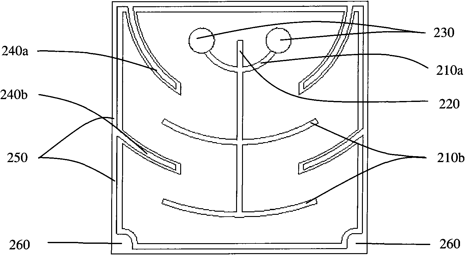
[0041] figure 2It is a schematic diagram of the second embodiment of the first LED electrode structure provided by the present invention. The first electrode includes first ring finger parts 210a and 210b, a first connecting part 220 connecting the first ring finger parts 210a and 210b, and at least one first contact part 230. The first electrode of the word "King". In this specific embodiment, two circular first contact portions 230 are located at the fingertip portion of the first ring finger portion 210a and form metal contact pads. It should be emphasized that the shape of the first contact portion 230 in this embodiment is not limited to a circle, and may also be a geometric figure such as an ellipse or a rectangle.

[0042] The second electrode includes two second ring finger portions 240 a and 240 b with different radii, a second connection portion 250 connecting the second ring finger portion 240 , and at least one second contact portion 260 . Wherein the second co...

Embodiment 3

[0046] image 3 It is a schematic diagram of Embodiment 3 of the third LED electrode structure provided by the present invention. The first electrode includes first ring finger parts 310a and 310b, first connecting parts 320a, 320b and 320c connecting the first ring finger parts 310a and 310b, and at least one first contact part 330. These three parts form a deformed ring shape. Bend "M" on the first electrode. In this specific embodiment, two circular first contact portions 330 are located in the middle of the ring finger of the first ring finger portion 310a and form metal contact pads. It should be emphasized that the shape of the first contact portion 230 in this embodiment is not limited to a circle, and may also be a geometric figure such as an ellipse or a rectangle.

[0047] The second electrode includes a second ring finger portion 340 , second connection portions 350 a , 350 b connecting the second ring finger portion 340 , and at least one second contact portion 3...


PUM


Abstract

The invention discloses an LED electrode structure, comprising a first electrode and a second electrode, wherein, the first electrode comprises at least two first ring finger parts, at least one first connection part and at least one first contact part; each first ring finger part is connected with the first connection part; the first contact part is arranged on the first ring finger part; the second electrode comprises at least two second ring finger parts, at least one second connection part and at least one second contact part; each second ring finger part is connected with the second connection part; the second contact part is inserted in the corner of the second connection part; the second electrode surrounds the first electrode in a closed manner and certain space exists between each part of the first electrode and the corresponding part of the second electrode. The LED electrode structure enables the distribution of the current of the light-emitting components and heating to be more uniform.

Description

technical field [0001] The invention relates to the field of semiconductor devices, and specifically discloses an LED electrode structure. Background technique [0002] In recent years, III-nitride materials and devices have become a research hotspot, especially nitride light-emitting diodes (LEDs). After continuous research and development, at present, the technology of growing nitrides using sapphire as a substrate has become mature and stable, and the technology of growing nitrides on Si substrates as a new substrate material is also gradually being developed. As one of the solid-state light-emitting elements, the main structure of the light-emitting diode includes a P-type semiconductor layer, an N-type semiconductor layer and a light-emitting layer between them. When the injection current is applied to the first contact layer included in the first electrode and the second contact layer included in the second electrode, holes in the P-type semiconductor layer and electr...

Claims


Application Information

Patent Timeline
IPC IPC(8): H01L33/00
Inventor 张佰君卫静婷王钢
Owner SUN YAT SEN UNIV
Why Eureka
Try Eureka