Liquid crystal device
A liquid crystal device, liquid crystal technology, applied in nonlinear optics, instruments, optics, etc., can solve the problem of high voltage
- Summary
- Abstract
- Description
- Claims
- Application Information
AI Technical Summary
Problems solved by technology
Method used
Image
Examples
example 1
[0144] Cells including bulk layers with hybrid orientation (HAN) and interdigitated electrodes
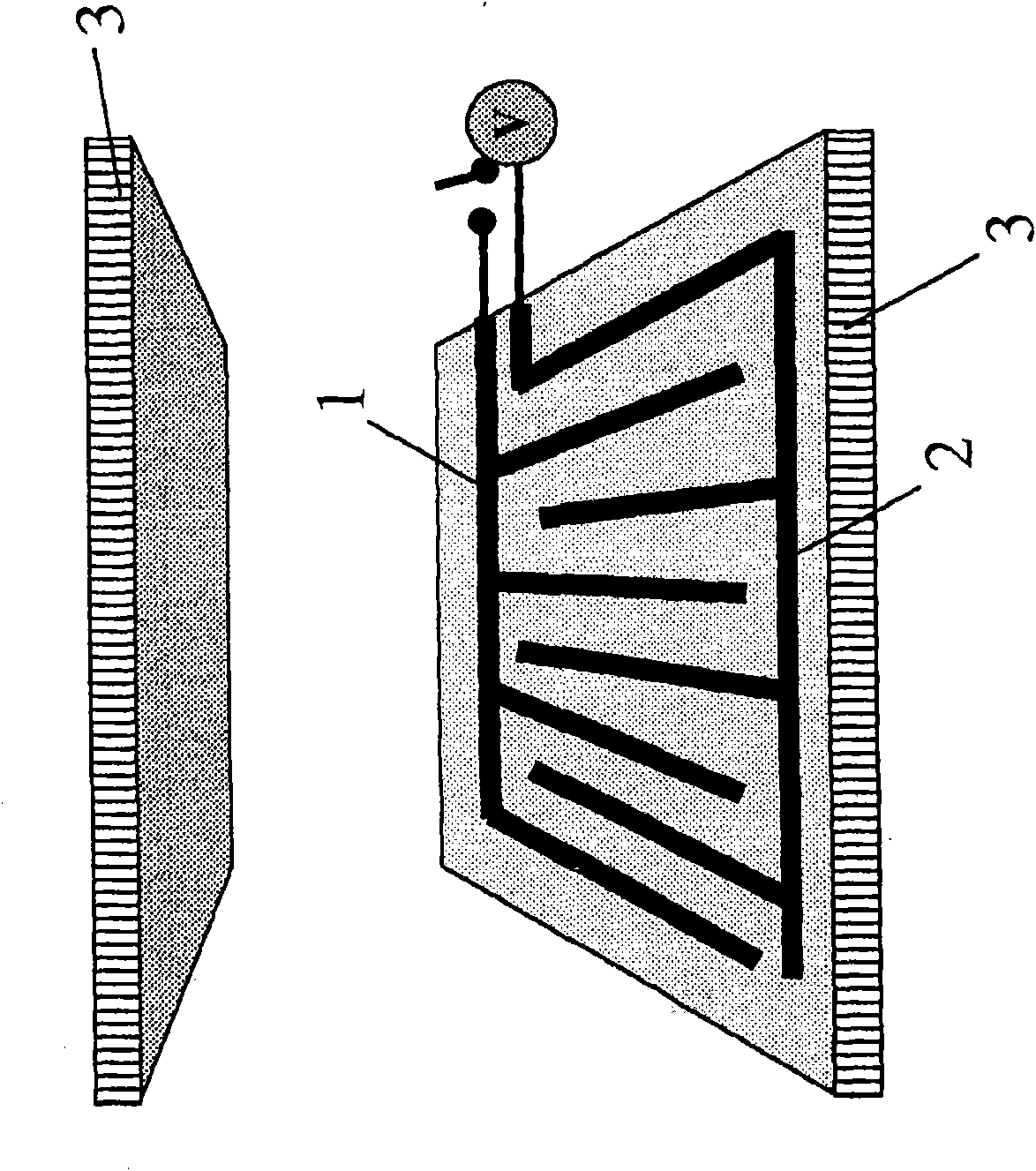
[0145] A sandwich cell including two parallel glass substrates 9 and 10 forming a cell gap of about 2 μm ( Picture 20 ). Interdigital electrode pattern 11 ( figure 1 Shown in) is disposed on the inner surface of one of the substrates 9 (single-sided device). The distance between adjacent electrodes is about 20 μm.
[0146] The first alignment layer 12 composed of Nissan SE-2170 is deposited on the electrode pattern 11 and rubbed parallel to the electrode pattern 11 to promote uniform planar alignment of the liquid crystal layer containing liquid crystal molecules 13 arranged in the cell gap .
[0147] A second alignment layer 14 composed of Nissan SE1211 that promotes vertical alignment is deposited on the inner surface of another substrate 10.
[0148] The cell gap is filled with a nematic liquid crystal material MLC 16000-000 (supplied by Merck) with positive dielectric anisotropy (...
example 2
[0154] Cells including bulk layers with hybrid orientation (HAN) and interdigitated electrodes
[0155] This example uses the same type of sandwich unit as Example 1, but the HAN structure is reversed ( Figure 26 ). Therefore, the orientation induced by the first orientation layer 18 at the substrate 15 carrying the electrode pattern 17 is vertical, and the orientation induced by the second orientation layer 20 at the opposite substrate 16 is planar. ,Such as Figure 26 with 27 Shown.
[0156] In addition, the cell is filled with another nematic liquid crystal material 19, MDA-05-187 (supplied by Merck) with negative dielectric anisotropy (Δε<0).
[0157] Because the bending deformation is localized at the substrate 15 carrying the electrode pattern 17 and because MDA-05-187 exhibits negative dielectric anisotropy, the strongest flexural electrical polarization is localized to the most obvious bending deformation Place, that is, at the substrate 15 carrying the electrode pattern ...
example 3
[0160] Including unit with chiral smectic orientation layer and interdigitated electrode
[0161] The unit used in this example ( Figure 32 ) Has the same structure as the unit used in Example 1. However, in this example, both inner surfaces of the substrates 21 and 22 are coated with an alignment layer (not shown) with Nissan SE-2170, which is rubbed unidirectionally along the electrode 23 to Promote a pretilt angle θ a The quasi-planar orientation.
[0162] On top of the alignment layer covering the electrode pattern 23, a thin film of ferroelectric liquid crystal polymer (FLCP), more specifically, a ferroelectric side chain polysiloxane (not shown) is deposited. FLCP layer has a molecular tilt angle θ b They are arranged in a book shelf shape, that is, the smectic layer is perpendicular to the substrate surface 21.
[0163] The cell gap is filled with an in-house prepared nematic liquid crystal material 24 that has negative dielectric anisotropy (Δε<0) and is immiscible (insol...
PUM
| Property | Measurement | Unit |
|---|---|---|
| thickness | aaaaa | aaaaa |
Abstract
Description
Claims
Application Information


