

Photoetching method and system
A technology of photolithography and photolithography technology, which is applied in the direction of micro-lithography exposure equipment, photolithography exposure device, electrical components, etc. Whether the engraving result is abnormal or not, so as to improve the efficiency of lithography
- Summary
- Abstract
- Description
- Claims
- Application Information
AI Technical Summary
Problems solved by technology
Method used
Image

Examples
Embodiment Construction
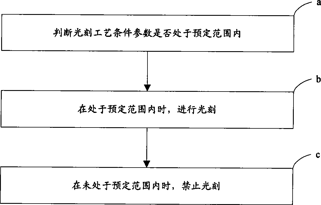
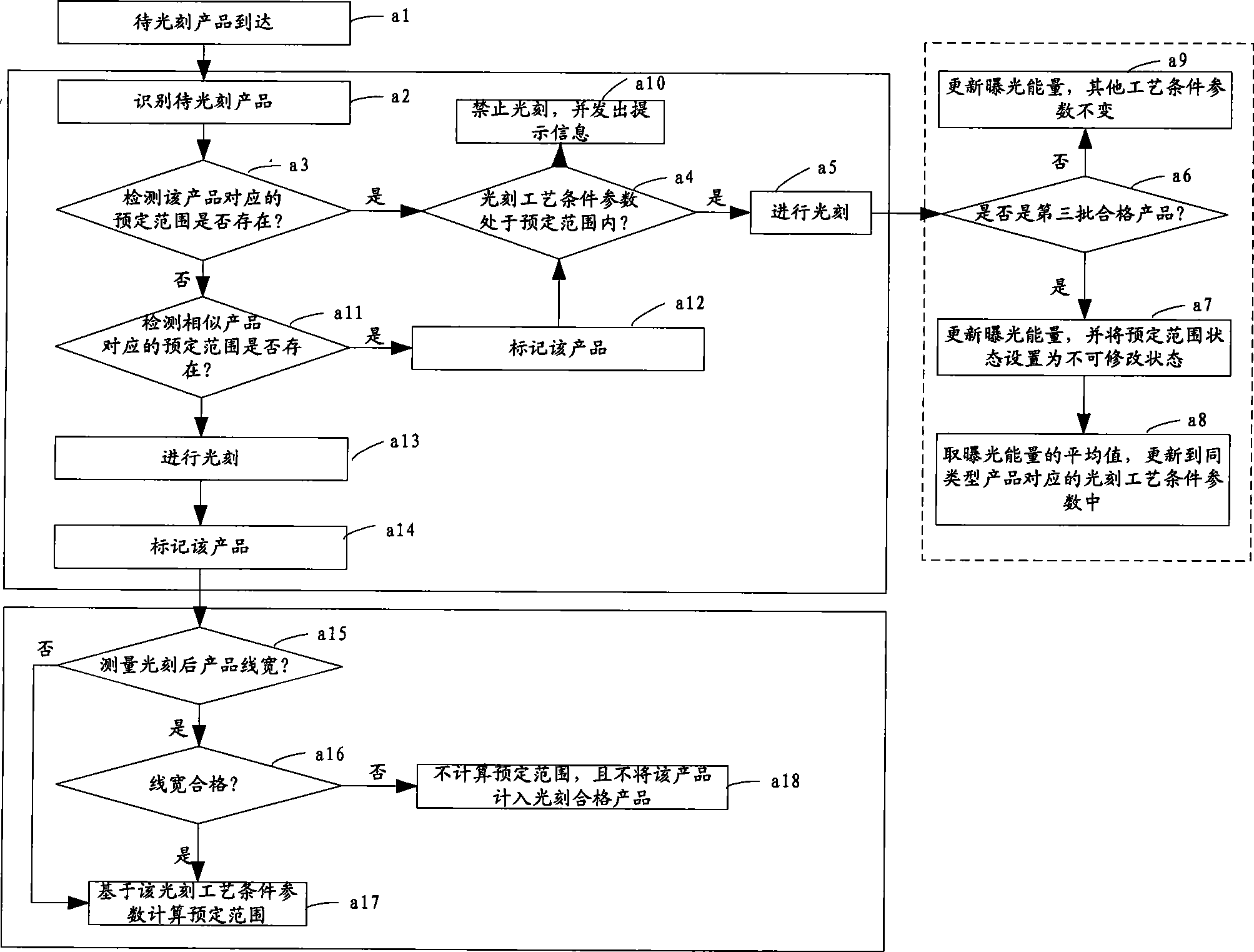
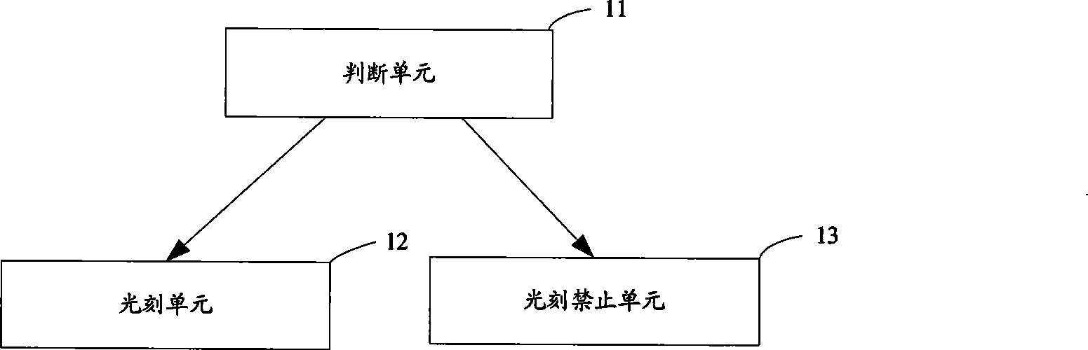
[0013] According to the analysis of the background technology, it can be seen that because the prior art may perform photolithography according to abnormal photolithography process condition parameters, the photolithography efficiency is reduced, so if the photolithography process condition parameters can be guaranteed to be reasonable, then it can be improved Lithography efficiency. Based on this consideration, the embodiment of the present invention proposes that the lithography efficiency can be improved through the following design idea: in the lithography process, based on the reasonable range of the lithography process condition parameters, it is judged whether the lithography process condition parameters can be used for lithography, if No, then the photolithography of the photolithography process conditions and parameters can be prohibited.
[0014] Based on the above design idea, the embodiment of the present invention proposes that the photolithography efficiency can ...
PUM
 Abstract
Description
Claims
Application Information