Front-end processed wafer having through-chip connections

A front-end processing and back-end processing technology, applied in the field of electrical connection, can solve problems such as useless chips, failure to make connections, discarding, etc., and achieve the effect of reducing cost impact and eliminating the risk of damage to devices

Active Publication Date: 2010-03-03
CUFER ASSET LTD LLC
View PDF23 Cites 3 Cited by
  • Summary
  • Abstract
  • Description
  • Claims
  • Application Information

AI Technical Summary

Problems solved by technology

[0004] One disadvantage of using through-chip vias on fully processed (i.e., device-bearing) chips is that the fully formed chip is significantly more expensive than the cost of a comparable blank wafer or partially processed chip
If errors are made in the alignment of the vias used for the electrical connection, it may damage the device on the chip or one or more metallization layers, or the desired connection cannot be made
[0005] In both cases, the result may be a useless chip that needs to be scrapped

Method used


Image

  • Front-end processed wafer having through-chip connections
  • Front-end processed wafer having through-chip connections
  • Front-end processed wafer having through-chip connections

Examples


Embodiment Construction

[0019] Serial numbers incorporated herein by reference as 11 / 329,481, 11 / 329,506, 11 / 329,539, 11 / 329,540, 11 / 329,556, 11 / 329,557, 11 / 329,558, 11 / 329,574, 11 / 329,575, 11 / 329,576, 5 US Patent Application 422,551 describes various techniques for forming small, deep vias in semiconductor wafers and electrical contacts for semiconductor wafers. Our technology allows for previously unavailable via densities and locations, and can be performed at chip or wafer scale.

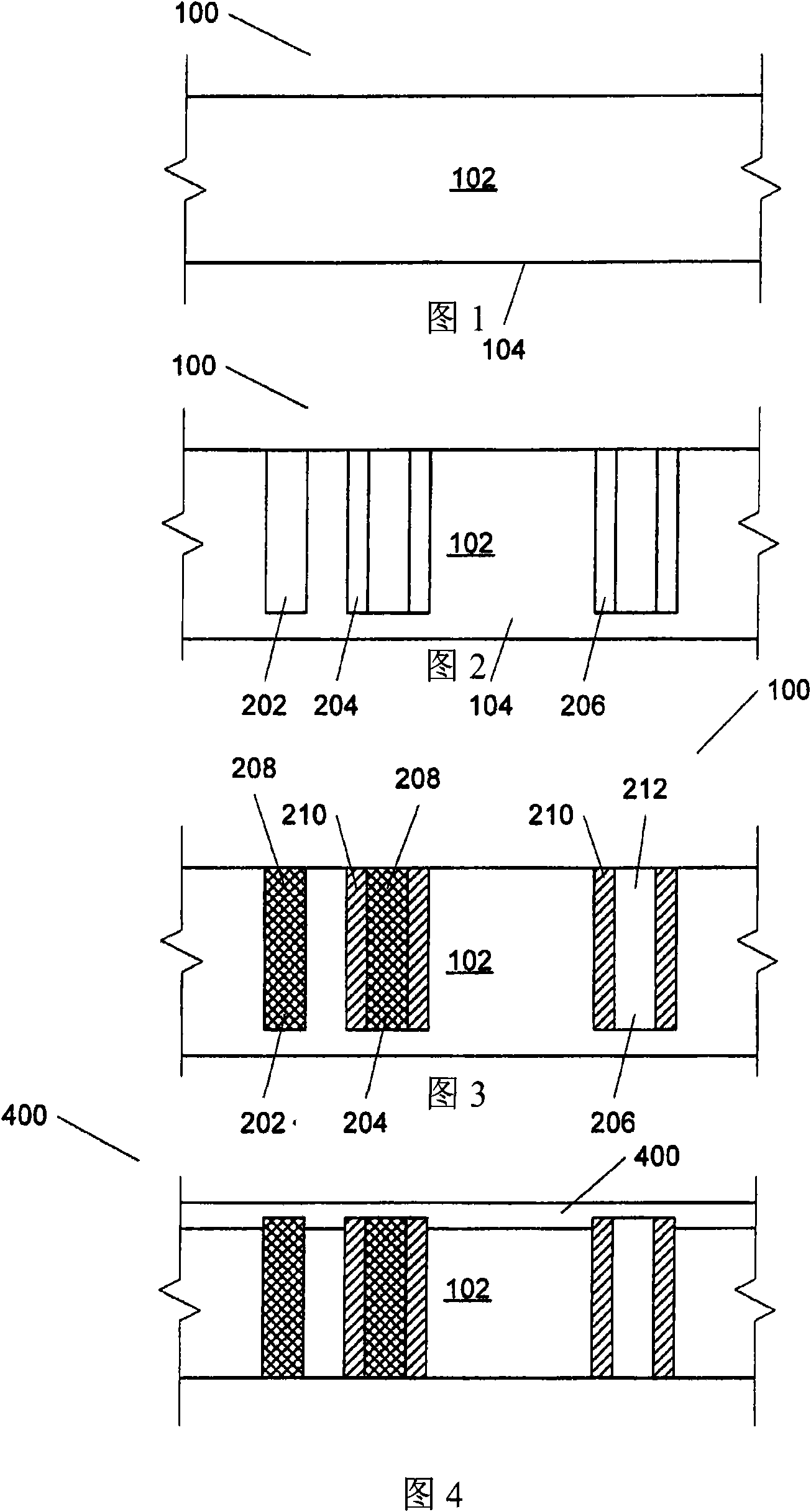
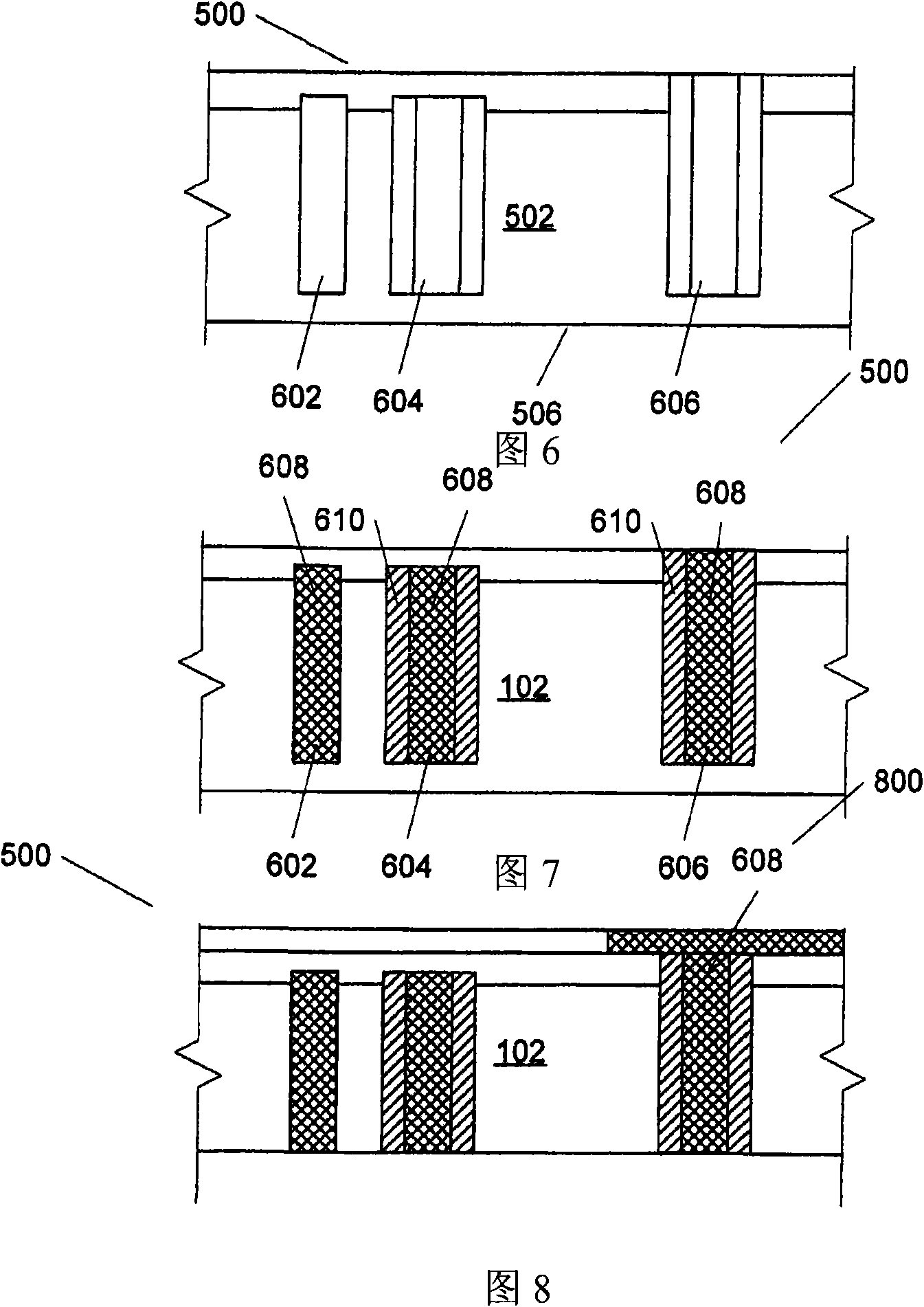
[0020] If it is desired to establish through-chip electrical connections, but minimize the risk involved in fully handling the wafer (ie, the device support wafer), the following approach can be used.

[0021] In summary, the method directly involves forming vias in a blank wafer at the locations where they should be associated with the devices that will be on the wafer once front-end processing is complete, making the vias conductive, and then fabricating the devices on the wafer, thereby utilizing Connections betwe...


PUM


Abstract

A method involves forming vias in a device-bearing semiconductor wafer, making at least some of the vias in the device-bearing semiconductor wafer electrically conductive, and performing back-end processing the device-bearing semiconductor wafer so as to create electrical connections between an electrically conductive via and a metalization layer. An alternative method involves forming vias in a device-bearing semiconductor wafer, making at least some of the vias in the device-bearing semiconductor wafer electrically conductive, and processing the device-bearing semiconductor wafer so as to create electrical connections between an electrically conductive via and a conductive semiconductor layer.

Description

technical field [0001] The present invention relates to semiconductors, and in particular to electrical connections for such devices. Cross References to Related Applications [0002] This application claims priority under 35 U.S.C. 119(e) to U.S. Provisional Application Serial No. 60 / 882,671, filed December 29, 2006, and also as U.S. Patent No. 11 / 422,551, filed June 6, 2006 A continuation of the application, the entire contents of which are hereby incorporated by reference as if fully set forth herein. Background technique [0003] It is often desirable to be able to make electrical connections across a chip in an efficient manner in order to connect it to another component. In most cases, this implies the use of vias and involves connections made near the devices of the chip, as opposed to connections formed on or near the periphery of the chip, as is done conventionally. [0004] One disadvantage of using through-chip vias on fully processed (ie, device-bearing) chip...

Claims


Application Information

Patent Timeline
Patent Type & Authority Applications(China)
IPC IPC(8): H01L21/4763H01L21/768
CPCH01L21/76898H01L23/481H01L2924/0002H01L2924/00H01L21/768
Inventor 约翰·特雷扎
Owner CUFER ASSET LTD LLC
Why Eureka
Try Eureka