Pulse width modulation control of a matrix converter
A matrix converter and modulation function technology, which is applied in the direction of converting AC power input to AC power output, converting equipment to DC without intermediate conversion, converting device of output power, etc., which can solve the complex control algorithm and increase the system Cost, consumption of processor resources, etc.
- Summary
- Abstract
- Description
- Claims
- Application Information
AI Technical Summary
Problems solved by technology
Method used
Image

Examples
Embodiment Construction
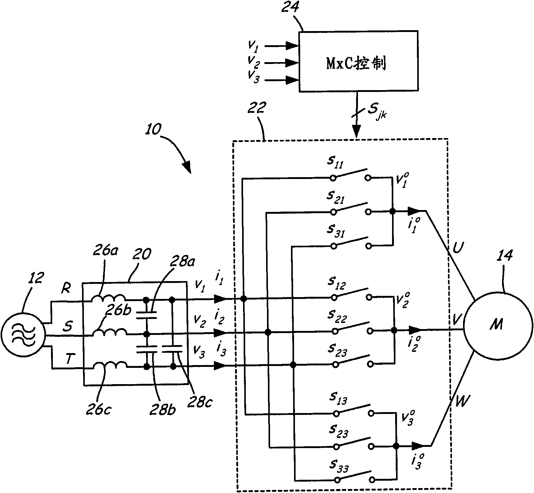
[0013] figure 1 is a schematic view of a power system 10 that receives multi-phase alternating current (AC) power at an input frequency from a power source 12 and provides the multi-phase AC power to a load at an output frequency. Power system 10 includes LC filter 20 , matrix converter 22 and matrix converter (MxC) controller 24 . In the illustrated embodiment, the power supply 12 is a three-phase power supply (comprising input phases R, S, and T) that provides an input voltage v at the input of a matrix converter 22 1 , v 2 and v 3 and provides an input current i 1 i 2 and i 3 . Also in this illustrated embodiment, the matrix converter 22 supplies the induction motor 14 with an output voltage v 1 o , v 2 o and v 3 o and output current i 1 o i 2 o and i 3 o Three-phase electricity (including U, V and W phases).
[0014] LC filter 20 includes inductors 26a, 26b, and 26c, and capacitors 28a, 28b, and 28c. The inductor 26a is connected in series with the inpu...
PUM
 Abstract
Description
Claims
Application Information
PatSnap Eureka turns technology decisions into work you can execute. Powered by our Innovation Knowledge Graph, it runs expert workflows across engineering, life sciences, materials and intellectual property. Get your review-ready output in minutes.


