Eureka AIR delivers breakthrough ideas for toughest innovation challenges, trusted by R&D personnel around the world.

Manipulator and wafer processing process

A technology of wafer processing and manipulators, applied in the direction of manipulators, conveyor objects, furnaces, etc., can solve problems that affect the process, easily generate vibration, damage wafers, etc., and achieve the effect of ensuring normal progress and protecting wafers

Active Publication Date: 2010-03-24
BEIJING NAURA MICROELECTRONICS EQUIP CO LTD
View PDF0 Cites 10 Cited by
  • Summary
  • Abstract
  • Description
  • Claims
  • Application Information

AI Technical Summary

Problems solved by technology

During the operation of the manipulator, the end effector 1 is prone to vibration, which causes friction between the wafer and the end effector 1, thereby generating particles, which will affect the process or damage the wafer

Method used


Image

  • Manipulator and wafer processing process
  • Manipulator and wafer processing process
  • Manipulator and wafer processing process

Examples


Embodiment Construction

[0017] Manipulator of the present invention, its preferred embodiment is as image 3 As shown, it includes a robotic arm 4 and an end effector 1. The front end of the robotic arm 4 is provided with a slot 6, and the rear end of the end effector 1 is inserted into the slot 6 to form a groove-mortise structure. Then, the mechanical arm 4 is fixedly connected to the end effector 1 . Due to the fixed connection of the groove-tenon structure, an integrated rigid connection structure is formed between the robot arm 4 and the end effector 1, which can reduce the vibration during the operation of the robot.

[0018] Specifically, the card slot 6 can be opened horizontally in the middle of the front end of the mechanical arm 4 , and the rear end of the end effector 1 is horizontally inserted into the card slot 6 . After the rear end of the end effector 1 is inserted into the card slot 6 , the mechanical arm 4 and the end effector 1 can be fixedly connected together by screws 2 . Ther...


PUM


Abstract

The invention discloses a manipulator and wafer processing process. The manipulator comprises a robot arm and an, wherein the front end of the robot arm is provided with a card slot, the rear end of the end actuator is inserted to the card slot, and is in fixedly connected through screws, to increase the integral rigidity, and further to reduce the vibration of the robot arm in the operation process; the upper surface of the end actuator is provided with a groove, plane shape of the groove is suitable for the plane shape of the processed wafer, the processed wafer can be put into the groove exactly, so as to hold the wafer at a fixed position in the motion period of the robot arm, and to enhance the wafer stability. The operation rate of the robot arm can be increased to increase the output of the wafer processing system in the unit time, the friction between the wafer and the end actuator is simultaneously avoided, to ensure the normal conducting of the processing technology, and toprotect the wafer.

Description

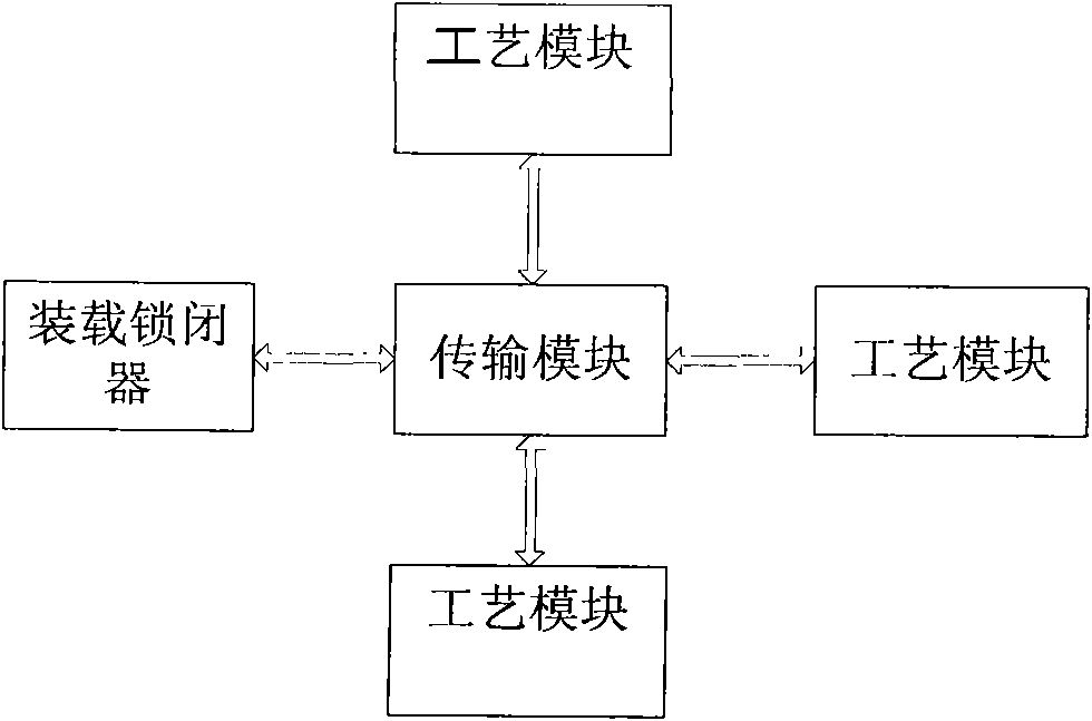
technical field [0001] The invention relates to a semiconductor processing equipment, in particular to a manipulator and a wafer processing system. Background technique [0002] In the manufacture of semiconductor devices (such as integrated circuits IC, dynamic random access memory DRAM), wafers for manufacturing semiconductor devices must often be transferred from one processing chamber of the wafer processing system to another processing chamber, and this transfer of wafers must be done in a dust-free environment. , in a vacuum environment. [0003] like figure 1 As shown, the wafer processing system in the prior art includes the following parts: load locker, transfer module, process module and so on. The manipulator is located in the transport chamber of the transport module, and the wafer is transported in the wafer processing system by the manipulator. [0004] The manipulator located in the transfer chamber consists of a robotic arm and an end effector. During the...

Claims


Application Information

Patent Timeline
Patent Type & Authority Applications(China)
IPC IPC(8): H01L21/677B65G47/90B65G49/07B25J15/00
Inventor 陈德高
Owner BEIJING NAURA MICROELECTRONICS EQUIP CO LTD
Why Eureka
Eureka Blog
Learn More