Active component array motherboard and manufacturing method thereof

A technology of active components and manufacturing methods, which is applied in the fields of electrical components, semiconductor/solid-state device manufacturing, and electrical solid-state devices, etc., can solve problems such as damage to lines or components, large electrode pad area of ​​the test pad structure, etc., to improve the process. The effect of yield

Inactive Publication Date: 2010-04-21
AU OPTRONICS CORP
View PDF0 Cites 8 Cited by
  • Summary
  • Abstract
  • Description
  • Claims
  • Application Information

AI Technical Summary

Problems solved by technology

[0004] However, in the above-mentioned array manufacturing process, the electrode pad area of ​​the test pad structure is often too large, and it is easy to be damaged in each manufacturing process step, such as the ion environment process of reactive ion etching (Reactive Ion Etching, RIE). , accumulate a large amount of charges on the electrode pads, so that the excessive charges will be introduced into the active device array due to the electrostatic discharge effect (ESD Effect), which will damage the lines or components in the active device array

Method used


Image

  • Active component array motherboard and manufacturing method thereof
  • Active component array motherboard and manufacturing method thereof
  • Active component array motherboard and manufacturing method thereof

Examples


Embodiment Construction

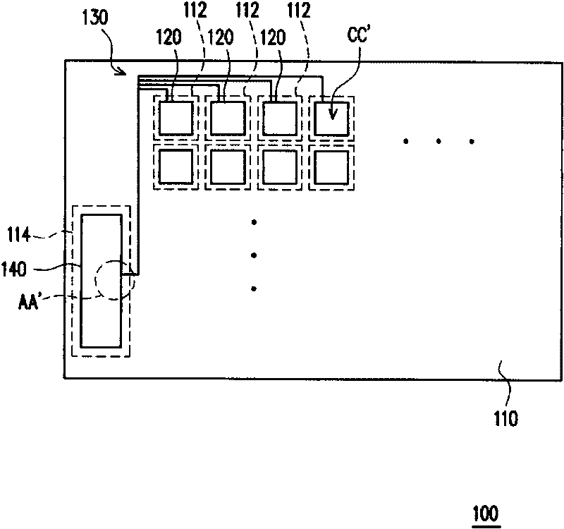
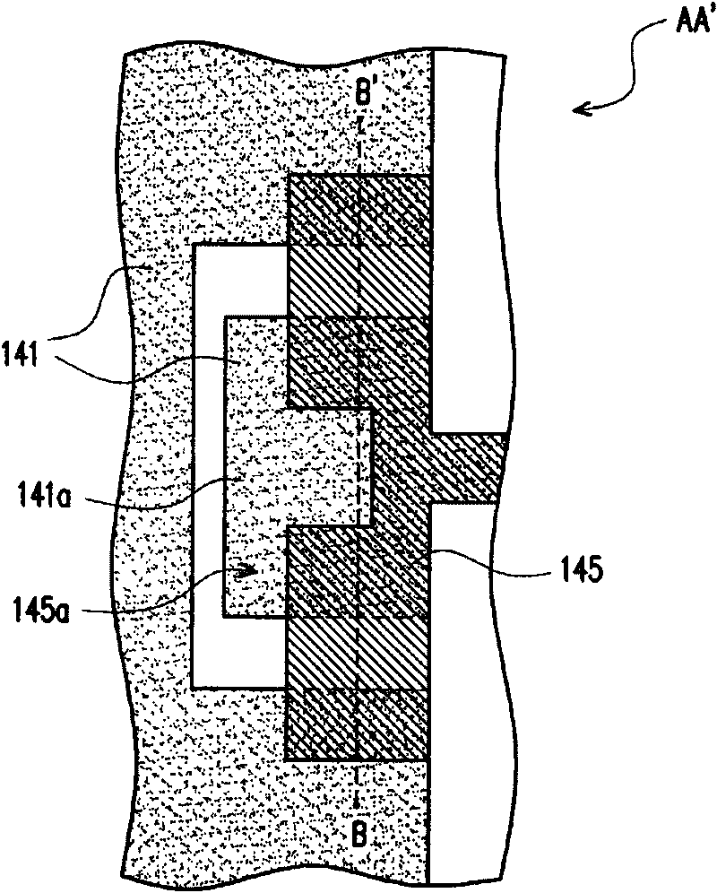
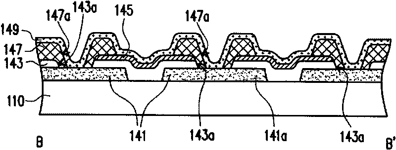
[0055]Generally speaking, because the electrode pad area of ​​the test pad structure is too large, a large amount of electrostatic charge is often accumulated on the electrode pad during the photolithography process. However, excessive electrostatic charge will be introduced into the active device array due to electrostatic discharge effect (ESD Effect), which will damage the circuits or elements in the active device array. In view of this, the present invention proposes an active device array motherboard, the test pad structure of which has a plurality of first metal patterns (that is, the above-mentioned electrode pads) that are separated from each other and electrically connected, so as to effectively reduce the size of the original electrode pads. area, thereby reducing static charge accumulation and preventing electrostatic discharge effects. The structure and implementation of the active device array mother substrate of the present invention will be described in detail b...


PUM


Abstract

The invention discloses an active component array motherboard, which comprises a substrate, a plurality of active component arrays, a connecting circuit and a testing pad structure. The substrate is provided with a plurality of predetermined areas and a peripheral area. The active component arrays are arranged in the predetermined areas respectively; the connecting circuit is arranged on the substrate; and the testing pad structure is arranged in the peripheral area and electrically connected to the active component arrays by the connecting circuit. The testing pad structure comprises a plurality of mutually separated first metal patterns which are electrically connected. The invention also provides a manufacturing method for the active component array motherboard.

Description

technical field [0001] The present invention relates to a mother substrate and a manufacturing method thereof, and in particular to an active element array mother substrate capable of effectively reducing electrostatic discharge (Electro-Static Discharge, ESD) effects and a manufacturing method thereof. Background technique [0002] Generally speaking, a liquid crystal display panel is mainly composed of an active device array substrate, a liquid crystal layer, and a color filter substrate. In the array process (array process), multiple active device arrays are usually fabricated on the mother substrate at the same time, and a test that is electrically connected to multiple active device arrays is directly fabricated on the mother substrate in the array process at the same time. The pad structure, wherein the test pad structure is electrically connected to a plurality of active device arrays through a connecting line, for example. [0003] After the above-mentioned array pr...

Claims


Application Information

Patent Timeline
Patent Type & Authority Applications(China)
IPC IPC(8): G02F1/1362G02F1/1368H01L21/82H01L23/544H01L23/60
Inventor 曹佩婷吴威宪陈静茹林圣智沈承勋
Owner AU OPTRONICS CORP
Why Eureka
Try Eureka