Surface light source device and liquid crystal display device assembly

A technology for liquid crystal display devices and surface light sources, which is applied to the components of lighting devices, lighting devices, optics, etc., and can solve problems such as uneven color

Inactive Publication Date: 2010-05-26
SONY CORP
View PDF2 Cites 9 Cited by
  • Summary
  • Abstract
  • Description
  • Claims
  • Application Information

AI Technical Summary

Problems solved by technology

This causes color unevenness to occur

Method used


Image

  • Surface light source device and liquid crystal display device assembly
  • Surface light source device and liquid crystal display device assembly
  • Surface light source device and liquid crystal display device assembly

Examples


no. 1 example

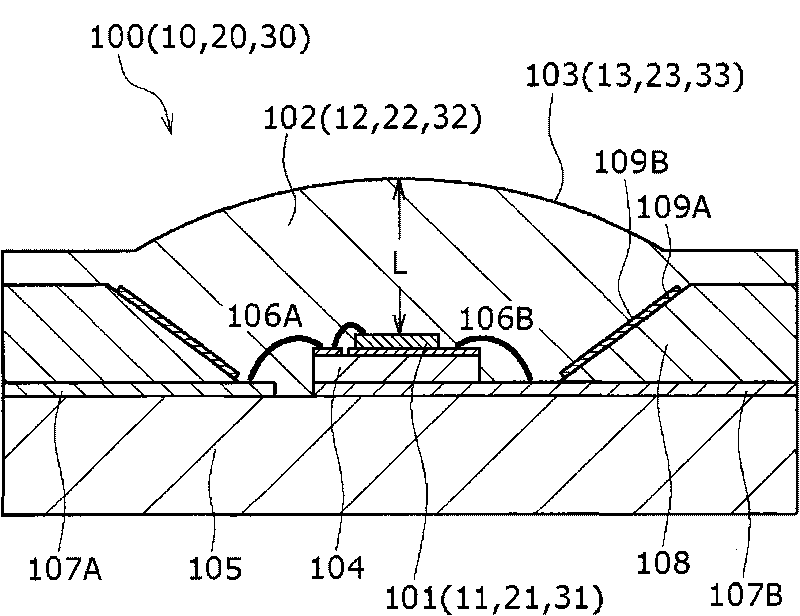
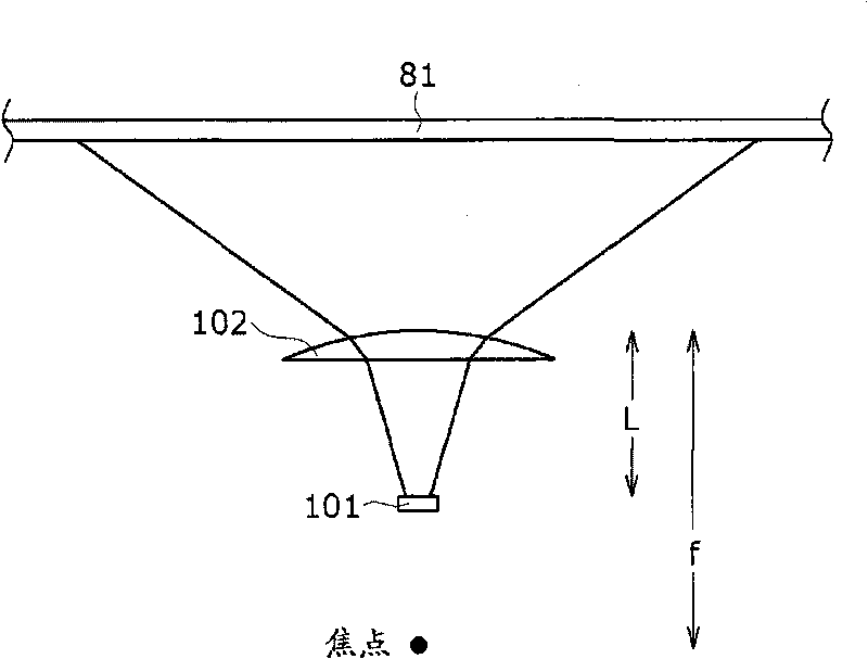
[0073] A first embodiment of the present invention relates to a surface light source device and a liquid crystal display device assembly according to the first and second embodiments of the present invention. The principle diagram of the liquid crystal display device assembly of the first embodiment is as follows figure 2 and image 3 shown. The schematic cross-sectional view of the light-emitting element assembly is shown in Figure 1A shown. A schematic partial end view of a liquid crystal display device assembly such as Figure 4 shown. A schematic partial end view of a liquid crystal display device such as Figure 5 shown.

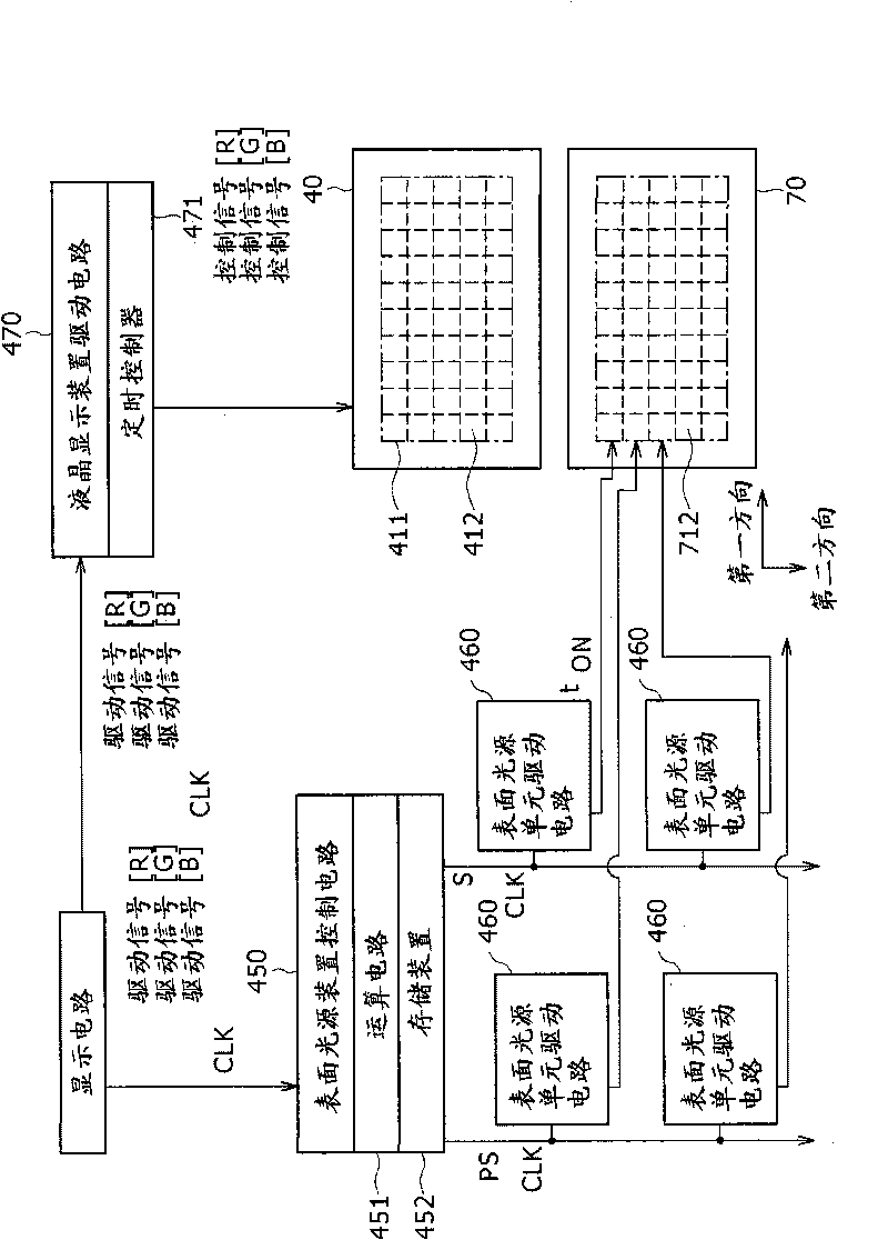
[0074] The surface light source device of the first embodiment illuminates a transmissive liquid crystal display device having a display area 411 formed of pixels arranged in a two-dimensional matrix from the backside thereof. further, such as figure 2 and image 3 As shown in the schematic diagram, the liquid crystal display device assembly ...

no. 2 example

[0159] The second embodiment of the present invention is a modification of the first embodiment. In the first embodiment, the light emitting element 101 is covered by the lens 102 without an intermediate gap therebetween. On the other hand, in the second embodiment, as Figure 11A As shown in the schematic cross-sectional view of , the light-emitting element 101 is opposite to the lens 102 with a light-transmitting medium layer 130 in between. Specifically, the recess 103A provided below the lower surface of the lens 102 is filled with the light-transmitting medium layer 130 . The light-transmitting medium layer 130 includes silicone gel resin (refractive index: 1.41), and the lens 102 includes polycarbonate resin with a refractive index of 1.59. Except for the above features, the same configuration and structure as the lens 102 and light emitting element assembly 100 in the first embodiment can be adopted as the configuration and structure of the lens 102 and light emitting...


PUM

PropertyMeasurementUnit
refractive indexaaaaaaaaaa

Abstract

Disclosed herein is a surface light source device that illuminates a transmissive liquid crystal display device having a display area formed of pixels arranged in a two-dimensional matrix from a back side of the liquid crystal display device, the surface light source device comprising a plurality of light emitting element units, wherein each of the light emitting element units includes: at least one first light emitting element assembly; at least one second light emitting element assembly; and at least one third light emitting element assembly, and focal length and lateral magnification of each of the first lens, the second lens, and the third lens are adjusted based on emission intensity distribution of each of the first light emitting element, the second light emitting element, and the third light emitting element.

Description

technical field [0001] The invention relates to a surface light source device and a liquid crystal display device component. Background technique [0002] In a liquid crystal display device, the liquid crystal material does not emit light. Therefore, for example, a direct surface light source device (backlight) for illuminating the display area of ​​the liquid crystal display device is arranged on the back side of the display area formed by a plurality of pixels. In a color liquid crystal display device, one pixel includes, for example, three types of sub-pixels: a red light-emitting sub-pixel, a green light-emitting sub-pixel and a blue light-emitting sub-pixel. By operating the liquid crystal cell of each sub-pixel as a kind of shutter (light valve), that is, by controlling the light transmittance (aperture ratio) of each sub-pixel to control the illumination light (such as white light) emitted from the surface light source device The light transmittance to display the i...

Claims


Application Information

Patent Timeline
Patent Type & Authority Applications(China)
IPC IPC(8): G02F1/13357F21V5/04
CPCG09G3/3426G09G2360/145G02F1/133603G09G2360/16G02F1/133609G02F2201/58G09G2300/023G09G2320/064G02F2001/133607G09G2320/0646G02F1/13318G02F1/133607
Inventor 植田充纪横沟宽治小日向真理子宫川祐一
Owner SONY CORP
Why Eureka
Try Eureka