Optical display with touch induction structure
An optical display and touch sensing technology, applied in optics, nonlinear optics, static indicators, etc., can solve problems such as heavy weight, contrary to the development trend of light, thin, and small displays, and the loss of flexible characteristics of electronic paper 14
- Summary
- Abstract
- Description
- Claims
- Application Information
AI Technical Summary
Problems solved by technology
Method used
Image

Examples
Embodiment Construction
[0031] In order to describe the structure, features and functions of the present invention in detail, the following preferred embodiments are given and described below with accompanying drawings.
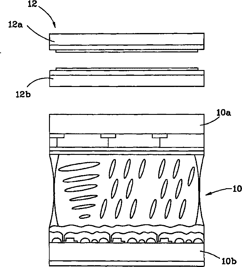
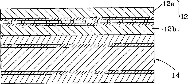
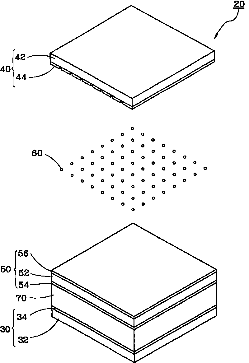
[0032] see Figure 3 to Figure 5 , is the optical display 20 provided by the first preferred embodiment of the present invention, which includes a thin film transistor array substrate 30, a pair of electrode substrates 40, an electrode plate 50, a plurality of spacers 60 and a display layer 70, wherein :
[0033] The thin film transistor array substrate 30 has a lower substrate 32 made of glass and an electrode surface 34 disposed on the surface of the lower substrate 32 .
[0034] The counter electrode substrate 40 is disposed above the thin film transistor array substrate 30, and has an upper substrate 42 made of polyethylene terephthalate (PET) and a plurality of stripes arranged side by side on the surface of the upper substrate 42. The first ITO electrode (Indium Tin Oxide fi...
PUM
 Abstract
Description
Claims
Application Information