Method for manufacturing liquid crystal display panel

A technology for liquid crystal display panels and manufacturing methods, which is applied to the photoplate-making process of patterned surfaces, optics, and optomechanical equipment, etc., and can solve problems such as color shift, multi-domain vertical alignment type liquid crystal display panel picture brightness changes, etc.

Inactive Publication Date: 2010-06-09
华映视讯(吴江)有限公司 +1
View PDF0 Cites 1 Cited by
  • Summary
  • Abstract
  • Description
  • Claims
  • Application Information

AI Technical Summary

Problems solved by technology

This will cause the image brightness of the multi-domain vertical alignment type liquid crystal display panel

Method used


Image

  • Method for manufacturing liquid crystal display panel
  • Method for manufacturing liquid crystal display panel
  • Method for manufacturing liquid crystal display panel

Examples


no. 1 example

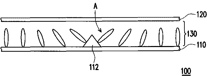
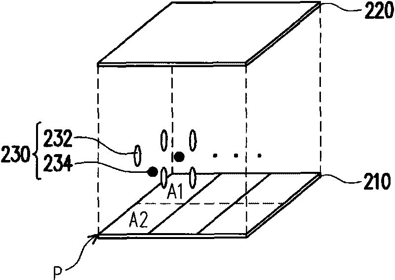
[0038] Figure 2A-2C It is a schematic flow chart of the manufacturing method of the liquid crystal display panel according to the first embodiment of the present invention. Please refer to Figure 2A Firstly, a first substrate 210 and a second substrate 220 are provided. Wherein the first substrate 210 has a plurality of pixels P. As shown in FIG. In particular, each pixel P can be divided into a first area A1 and a second area A2, Figure 2A are shown as two regions, but not limited thereto). In other embodiments, each pixel P can be divided into more than two regions, such as three, four or more regions. In practice, the first substrate 210 is, for example, an active device array substrate, and the second substrate 220 is a color filter substrate. In other embodiments, the first substrate 210 can also be an active device array substrate (manufactured by COA technology) with a color filter layer, and the second substrate 220 is a transparent substrate with a shared elec...

no. 2 example

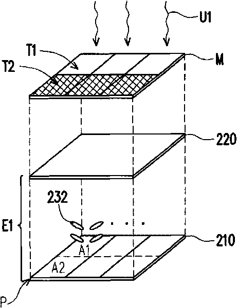
[0044] The second embodiment is similar to the first embodiment, and the similarities will not be repeated here. The main difference between the two is: the position of the mask during the exposure process. Figure 4A is the position of the photomask in the first light irradiation step in the second embodiment of the present invention. Such as Figure 4A As shown, the photomask M may be located under the first substrate 210 for exposure. Wherein, the light-transmitting area T1 of the mask M corresponds to the first area A1.

[0045] Figure 4B is the position of the photomask in the second light irradiation step of the second embodiment of the present invention. Please refer to Figure 4B , the mask M is located above the first substrate 210 . Wherein, the light-transmitting area T1 of the mask M corresponds to the second area A2. This also enables the first light irradiation step and the second light irradiation step to proceed smoothly, so that the liquid crystal mole...


PUM


Abstract

The invention discloses a method for manufacturing a liquid crystal display panel, which comprises: firstly, providing a first substrate and a second substrate, wherein the first substrate has a plurality of pixels and each pixel at least has a first area and a second area; secondly, forming mixed solution between the first substrate and the second substrate; thirdly, forming a first electric field between the first substrate and the second substrate; fourthly, performing primary light irradiation of the mixed solution corresponding to the first area to offer the liquid crystal molecules in the first area a first pretilt angle; and fifthly, forming a second electric field between the first substrate and the second substrate and performing secondary light irradiation of the mixed solution corresponding to the second area to offer the liquid crystal molecules in the second area a second pretilt angle.

Description

technical field [0001] The present invention relates to a method for manufacturing a liquid crystal display panel, and in particular to a method for manufacturing a liquid crystal display panel using PSA (Polymer Sustain Alignment) technology. Background technique [0002] The multimedia technology in today's society is quite developed, mostly benefiting from the progress of semiconductor components and display devices. As far as displays are concerned, liquid crystal display panels with superior characteristics such as high image quality, good space utilization efficiency, low power consumption, and no radiation have gradually become the mainstream of the market. [0003] figure 1 It is a schematic cross-sectional view of a known multi-domain vertical alignment liquid crystal display panel. Please refer to figure 1 , the known multi-domain vertical alignment liquid crystal display panel 100 includes a thin film transistor array substrate 110, a color filter substrate 120...

Claims


Application Information

Patent Timeline
IPC IPC(8): G02F1/1333G03F7/00
Inventor 刘纯秀庄嘉玲
Owner 华映视讯(吴江)有限公司
Why Eureka
Try Eureka