Display substrate, preparation method of display substrate, and display device
A technology for display substrates and display devices, applied in instruments, semiconductor devices, optics, etc., can solve the problems of liquid crystal molecular orientation disorder, lack of viewing angle compensation, and large birefringence, so as to achieve improved picture quality and good viewing angle experience , Excellent wide viewing angle display effect
- Summary
- Abstract
- Description
- Claims
- Application Information
AI Technical Summary
Problems solved by technology
Method used
Image
Examples
Embodiment 1
[0038] This embodiment provides a display substrate, which has a better effect of anchoring the alignment of liquid crystals, so better display quality can be obtained.
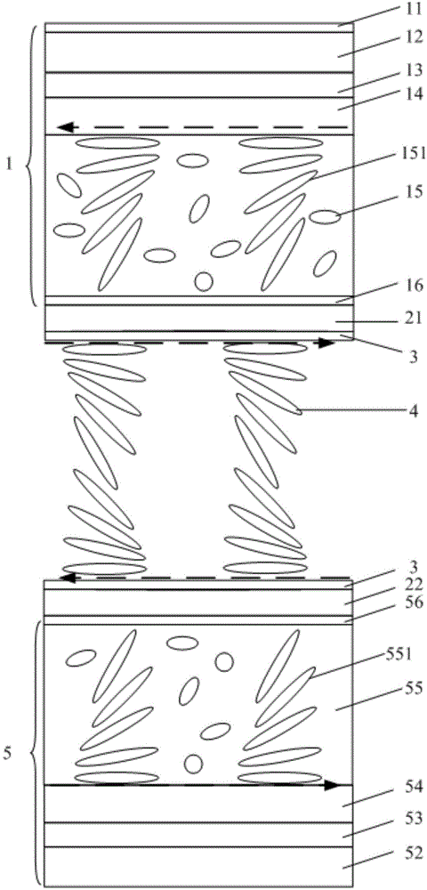
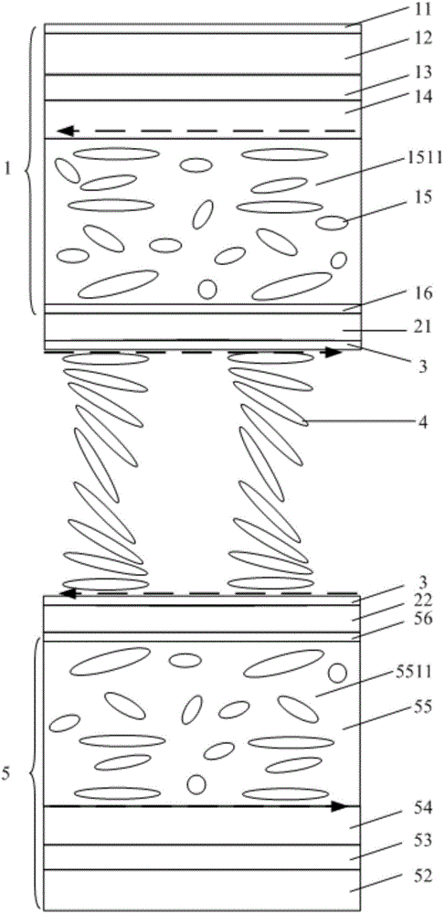
[0039] Such as Figure 4 As shown, the display substrate includes a color filter substrate 21, an array substrate 22, and a liquid crystal layer arranged between the color filter substrate 21 and the array substrate 22, and a side of the color filter substrate 21 and the array substrate 22 facing the liquid crystal layer Alignment layers 3 are respectively provided on the sides, and a viewing angle compensation layer is also included between the color filter substrate 21 and the alignment layer 3, and between the array substrate 22 and the alignment layer 3.
[0040] Wherein, the viewing angle compensation layer is formed of RM (Reactive Mesogens, active radical) material. At present, RM materials are mainly developed by Merck. A typical RM material is a reactive azobenzene liquid crystal material, which has...
Embodiment 2
[0058] This embodiment provides a display device, including the display substrate in Embodiment 1.
[0059] The display device may be any product or component with a display function, such as a liquid crystal panel, electronic paper, a mobile phone, a tablet computer, a television set, a monitor, a notebook computer, a digital photo frame, a navigator, and the like.
[0060] The display device utilizes the property of RM material to fix the polymerized liquid crystal phase, and compensates the display viewing angle by fabricating it in the display substrate. Compared with the current technical means of fabricating DLC film in the polarizer substrate outside the liquid crystal cell, it can Avoiding the latter’s hourglass mura display defects caused by the disordered arrangement of liquid crystal molecules in the DLC layer in the polarizer substrate under high temperature, high humidity or thermal shock conditions, and to a certain extent improve the performance of liquid cryst...
PUM
| Property | Measurement | Unit |
|---|---|---|
| thickness | aaaaa | aaaaa |
Abstract
Description
Claims
Application Information
 - R&D
- Intellectual Property
- Life Sciences
- Materials
- Tech Scout
- Unparalleled Data Quality
- Higher Quality Content
- 60% Fewer Hallucinations
Browse by: Latest US Patents, China's latest patents, Technical Efficacy Thesaurus, Application Domain, Technology Topic, Popular Technical Reports.
© 2025 PatSnap. All rights reserved.Legal|Privacy policy|Modern Slavery Act Transparency Statement|Sitemap|About US| Contact US: help@patsnap.com


