Method for gate oxide integrity (GOI) test of MOS transistor devices
A MOS transistor and gate oxide technology, applied in the field of MOS transistor device gate oxide integrity testing, can solve problems such as accurately reflecting the specific conditions of the gate oxide, device failure analysis, and inability to spend time.
- Summary
- Abstract
- Description
- Claims
- Application Information
AI Technical Summary
Problems solved by technology
Method used
Image

Examples
Embodiment Construction
[0023] In order to make the technical features of the present invention more comprehensible, specific embodiments are given below in conjunction with the accompanying drawings to further describe the present invention.
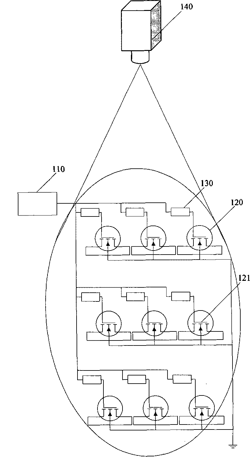
[0024] See figure 1 , which shows a schematic diagram of a system for testing the integrity of the gate oxide layer of a MOS transistor device provided by an embodiment of the present invention. The testing system includes:
[0025] A test power supply 110, a plurality of MOS transistor devices 120 to be tested are respectively connected to the test power supply 110, in this embodiment, the MOS transistor devices 120 to be tested are respectively connected by an electric programmable fuse (eFUSE electrically programmable fuse device) 130 The test power supply 110 is used to form a parallel gate oxide integrity (GOI) test system. The detection device 140 is configured to detect failure points on the MOS transistor device 120 .
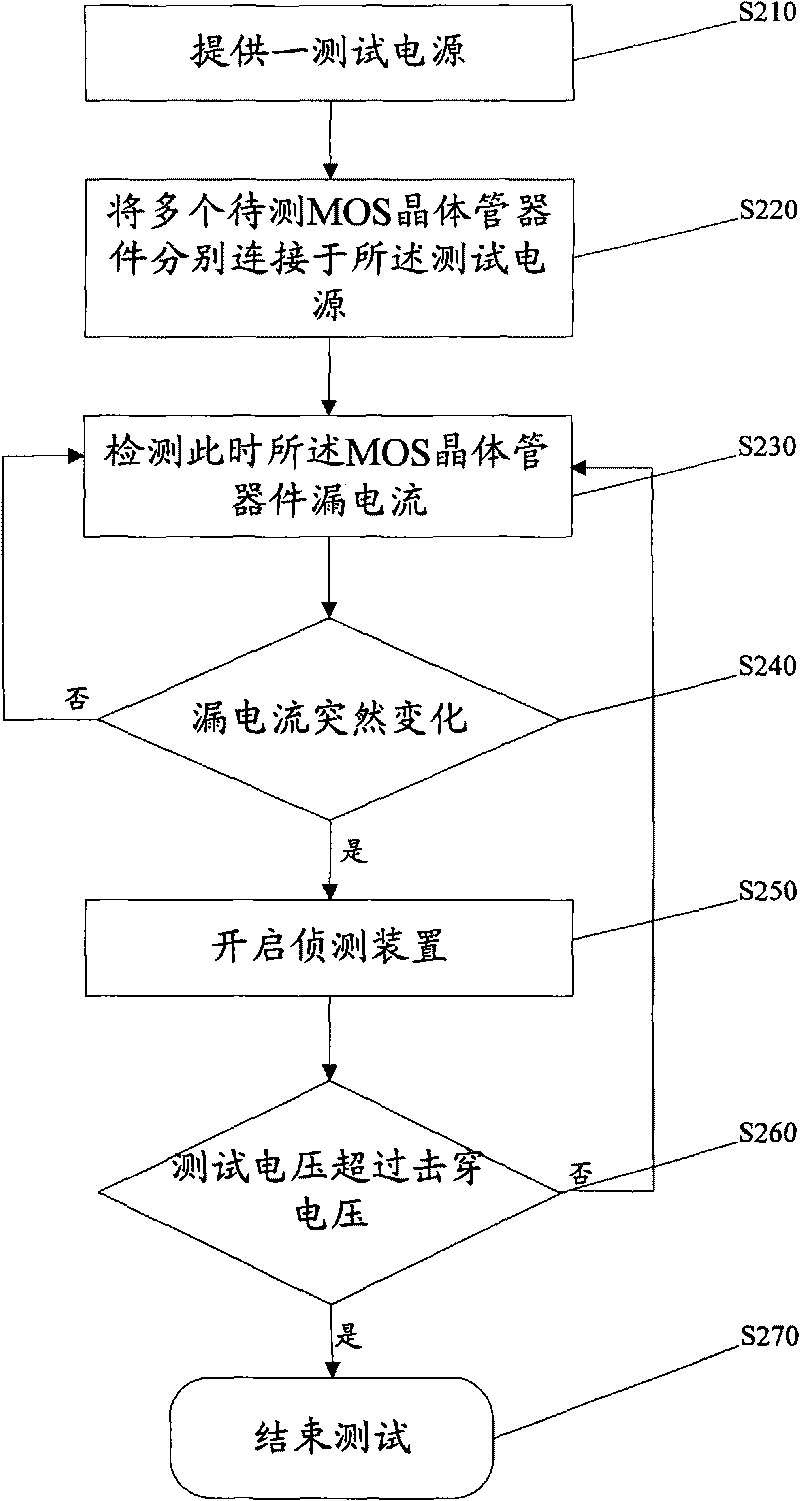
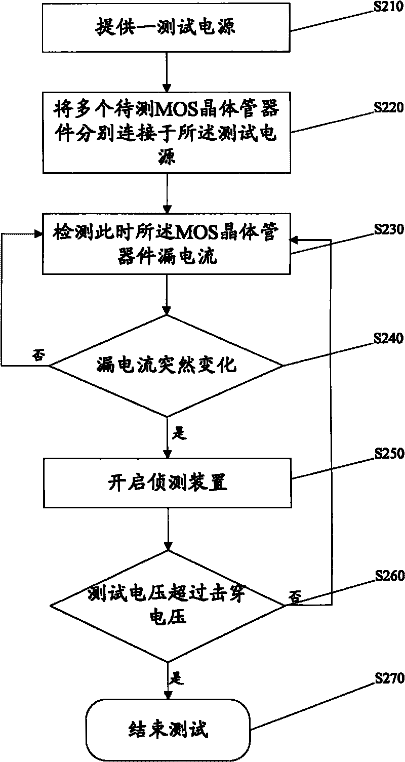
[0026] See figure 2 , which ...
PUM
 Abstract
Description
Claims
Application Information
 - R&D
- Intellectual Property
- Life Sciences
- Materials
- Tech Scout
- Unparalleled Data Quality
- Higher Quality Content
- 60% Fewer Hallucinations
Browse by: Latest US Patents, China's latest patents, Technical Efficacy Thesaurus, Application Domain, Technology Topic, Popular Technical Reports.
© 2025 PatSnap. All rights reserved.Legal|Privacy policy|Modern Slavery Act Transparency Statement|Sitemap|About US| Contact US: help@patsnap.com