Coupling layer and printed circuit board with same

A technology of printed circuit board and coupling layer, applied in the direction of printed circuit, printed circuit, printed circuit components, etc., can solve the problems of large area of ​​printed circuit board, small area of ​​power layer 20 can not meet the design requirements, etc., to suppress electromagnetic radiation Effect

Inactive Publication Date: 2010-06-09
HONG FU JIN PRECISION IND (SHENZHEN) CO LTD +1
View PDF0 Cites 5 Cited by
  • Summary
  • Abstract
  • Description
  • Claims
  • Application Information

AI Technical Summary

Problems solved by technology

However, along with the miniaturization trend of electronic products, the power layer 20 of the printed circuit board will be retracted by a certain distance, which will inevitably cause the area of ​​the power layer 20 to be too small to meet the design requirements; if the area of ​​the ground layer 30 is increased to increase the power layer 20 Relative to the indentation distance of the formation 30, the area of ​​the printed circuit board will be too large

Method used


Image

  • Coupling layer and printed circuit board with same
  • Coupling layer and printed circuit board with same
  • Coupling layer and printed circuit board with same

Examples


Embodiment Construction

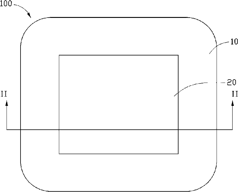
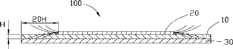
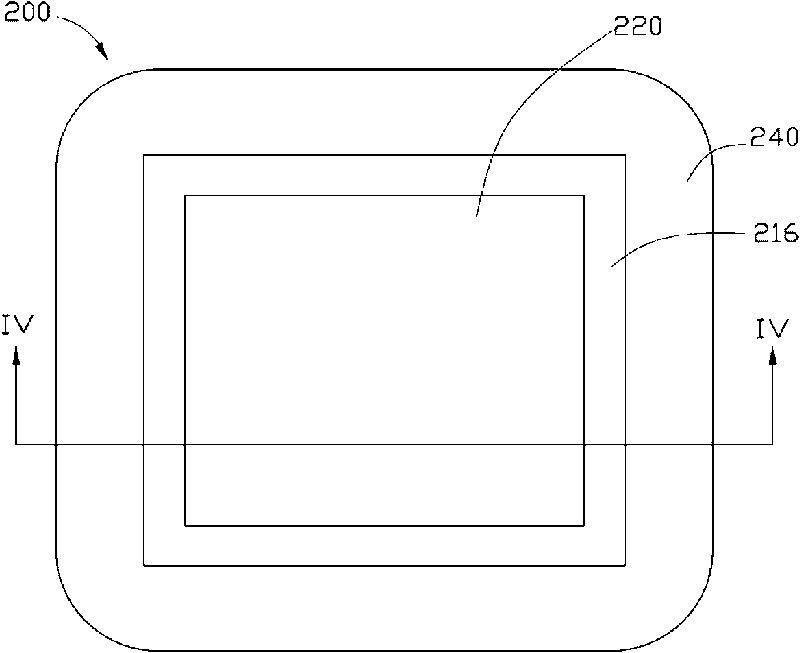
[0014] combine image 3 and Figure 4 , the present invention provides a coupling layer 200 for a printed circuit board, which includes: a first dielectric layer 210 , a power layer 220 and a ground layer 230 . The first dielectric layer 210 includes a first surface 212 and a second surface 214 opposite to the first surface 212 . The power layer 220 and the ground layer 230 cover the first surface 212 and the second surface 214 respectively. The thickness of the first dielectric layer 210 is H. On the first surface 212 , the power layer 220 is indented a distance from the ground layer 230 to form a bare area 216 . Preferably, the distance is selected as 20H. It can be understood that the distance can also be greater than 20H. The coupling layer 200 also includes a via hole 250 . The exposed area 216 is covered with a conductive layer 240 insulated from the power layer 220 , and the conductive layer 240 is electrically connected to the ground layer 230 through the via hol...


PUM


Abstract

The invention provides a coupling layer used for printed circuit boards. The coupling layer comprises a first dielectric layer, a power layer and a ground layer, wherein the first dielectric layer comprises a first surface and a second surface opposite to the first surface; the power layer and the ground layer are arranged on the first surface and the second surface respectively; the power layer on the first surface retracts by a certain distance relative to the ground layer so as to form a bare area; a conducting layer insulated from the power layer is arranged on the bare area; and the conducting layer is electrically connected with the ground layer so as to further inhibit electromagnetic radiation generated by the power layer. The invention also provides a printed circuit board having the coupling layer.

Description

technical field [0001] The invention relates to a coupling layer and a printed circuit board with the coupling layer. Background technique [0002] Due to the continuous improvement and updating of electronic products, the demand for functions and efficiency continues to increase. It is the most direct way to increase the frequency of work to increase the efficiency of products. Just like the frequency of the CPU of the computer is constantly doubling every year, the work is constantly getting faster. The electromagnetic radiation interference problem caused by the indirect increase in frequency can be solved in many ways to improve the electromagnetic radiation interference, and the improvement of the printed circuit board (PCB) layout (Layout placement) is one of them. combine figure 1 and figure 2 , the printed circuit board (not shown) in the prior art includes a coupling layer 100 . The coupling layer 100 includes a power layer 20 , a dielectric material layer 10 an...

Claims


Application Information

Patent Timeline
Patent Type & Authority Applications(China)
IPC IPC(8): H05K1/02H05K1/03H05K3/46
CPCH05K2201/09309H05K2201/09345H05K2201/09618H05K1/0218H05K2201/09354H05K2201/0715
Inventor 范发平
Owner HONG FU JIN PRECISION IND (SHENZHEN) CO LTD
Why Eureka
Try Eureka