
Silicon wafer transferring arm and use method thereof

An arm, silicon wafer technology, applied in the field of silicon wafer transfer arm, can solve the problem of not being able to transfer silicon wafers at the same time

Active Publication Date: 2011-11-02
SHANGHAI HUAHONG GRACE SEMICON MFG CORP
View PDF0 Cites 0 Cited by
  • Summary
  • Abstract
  • Description
  • Claims
  • Application Information

AI Technical Summary

Problems solved by technology

[0002] At present, the silicon wafer transfer arm used in the manufacturing process of integrated circuits cannot simultaneously transfer silicon wafers to multiple directions (such as horizontal and vertical directions). If it is necessary to transfer silicon wafers to multiple directions, multiple independent The arms are used step by step and cannot be done on the same arm

Method used


Image

  • Silicon wafer transferring arm and use method thereof
  • Silicon wafer transferring arm and use method thereof
  • Silicon wafer transferring arm and use method thereof

Examples


Embodiment Construction

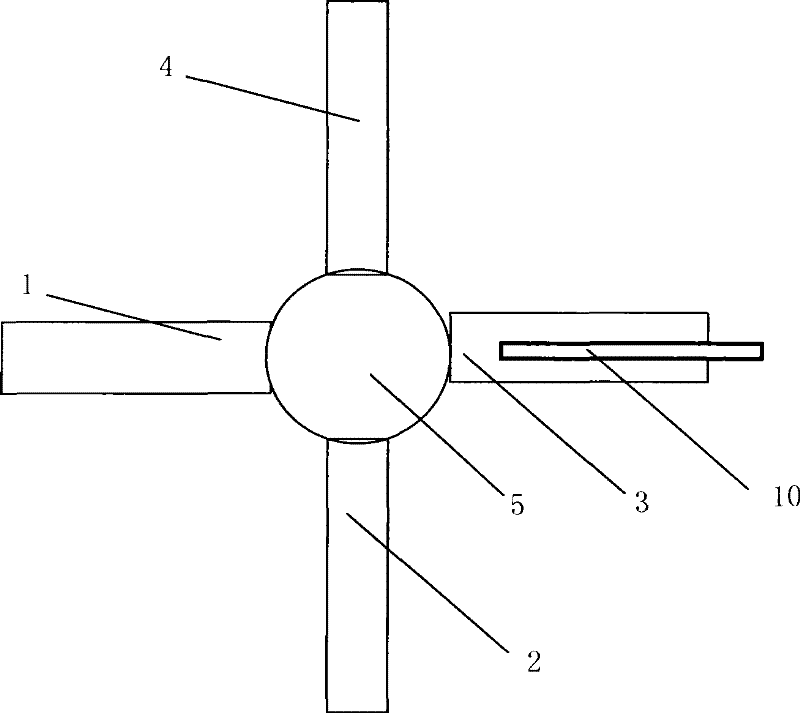
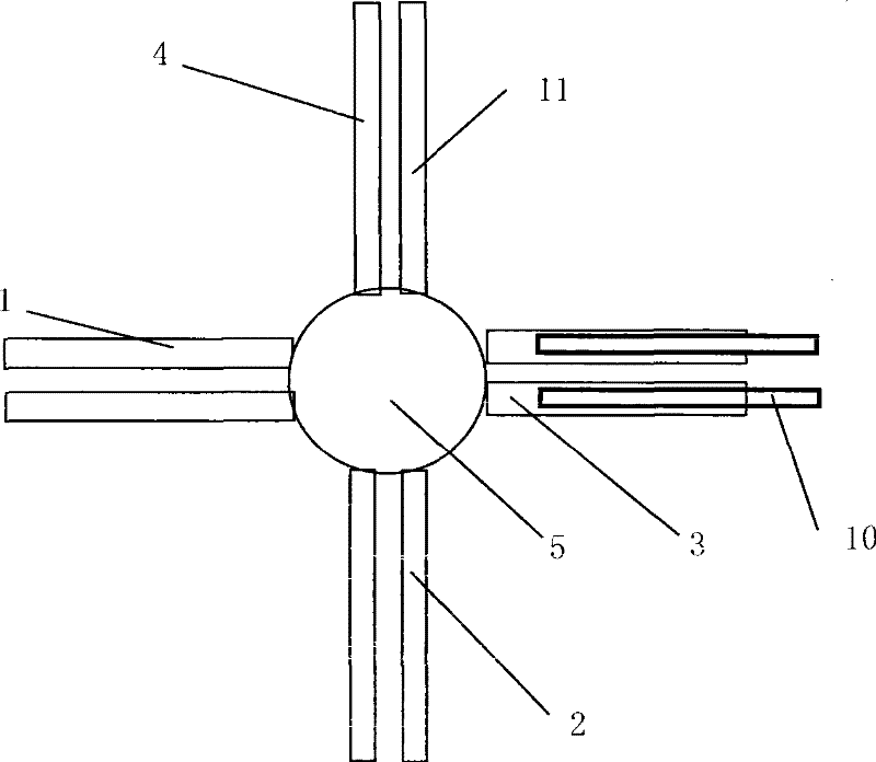
[0024] Such as figure 1 As shown, the silicon wafer transfer arm of the present invention includes arm supports 1, 2, 3, 4, which are respectively fixedly connected to the connector 5, and the arm supports 1, 2, 3, 4 form a cross shape with each other. The connector 5 is connected with the rotation control shaft, and the rotation control shaft is connected with the driving motor. The drive motor controls the rotation of the connector 5 by driving the rotation of the rotation control shaft.

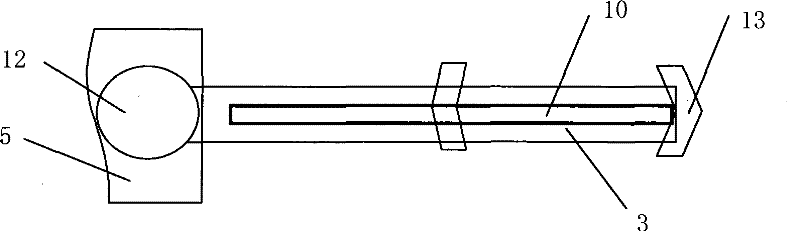
[0025] Such as image 3 , Figure 4 As shown, each arm bracket includes two clamping handles 11, and the two clamping handles 11 form a scissors shape, so that the arm bracket becomes a clamp that can be opened and closed. The curvature of the edge of the silicon wafer 10 is suitable. The silicon wafer 10 can be clamped along the circular edge of the silicon wafer 10 when the clips are closed.

[0026] The arc portion of the clamping handle 11 is fixedly provided with a plurality of s...


PUM


Abstract

The invention discloses a silicon wafer transferring arm which comprises a plurality of arm brackets, a connector and a driving motor, wherein one end of each arm bracket is connected with the connector; the connector is connected with the driving motor; the number of the arm brackets is four, and the four arm brackets form cross shapes with each other; the arm brackets in the horizontal direction are used for receiving and sending the silicon wafers in the horizontal direction; the arm brackets in the vertical direction are used for transferring the silicon wafers in the vertical direction; the arm bracket at the right side is used for receiving the silicon wafers; the arm bracket at the lower side is used for transferring in the vertical direction; the arm bracket at the left side is used for sending the silicon wafers; and under the rotational driving of a rotational control shaft, the arm brackets in the horizontal direction and the vertical direction can realize function exchange. The invention can carry out silicon wafer transferring operation in a plurality of directions in one arm and simultaneously transfer the silicon wafers in the horizontal direction and the vertical direction. The invention also discloses a use method of the silicon wafer transferring arm.

Description

technical field [0001] The invention relates to a semiconductor manufacturing device, in particular to a silicon wafer transfer arm, and also relates to a method for using the silicon wafer transfer arm. Background technique [0002] At present, the silicon wafer transfer arm used in the manufacturing process of integrated circuits cannot simultaneously transfer silicon wafers to multiple directions (such as horizontal and vertical directions). If it is necessary to transfer silicon wafers to multiple directions, multiple independent The arms are used in steps to work together and cannot be done on the same arm. Contents of the invention [0003] The technical problem to be solved by the present invention is to provide a silicon wafer transfer arm, which can transfer silicon wafers to multiple directions at the same time. [0004] In order to solve the above technical problems, the technical solution of the silicon wafer transfer arm of the present invention is: [0005]...

Claims


Application Information

Patent Timeline
Patent Type & Authority Patents(China)
IPC IPC(8): H01L21/677
Inventor 宁开明
Owner SHANGHAI HUAHONG GRACE SEMICON MFG CORP
Learn More