Method for manufacturing aluminum wiring

A manufacturing method and aluminum wiring technology, applied in semiconductor/solid-state device manufacturing, electrical components, circuits, etc., can solve problems that affect the quality of semiconductor devices, and achieve the effect of avoiding quality

Active Publication Date: 2012-05-16
SEMICON MFG INT (SHANGHAI) CORP
View PDF1 Cites 0 Cited by
  • Summary
  • Abstract
  • Description
  • Claims
  • Application Information

AI Technical Summary

Problems solved by technology

[0008] The problem to be solved by the present invention is that there are etching defects in the existing aluminum wiring process, which affects the quality of semiconductor devices

Method used


Image

  • Method for manufacturing aluminum wiring
  • Method for manufacturing aluminum wiring
  • Method for manufacturing aluminum wiring

Examples


Embodiment approach

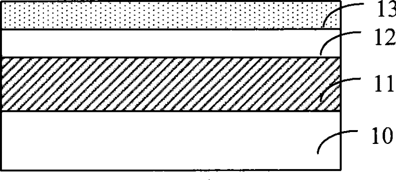
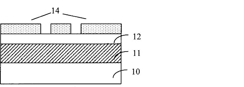
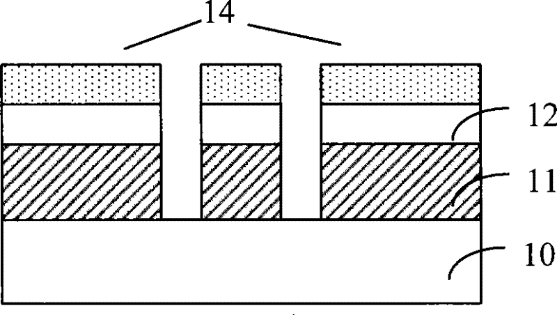
[0022] In view of this, an embodiment of the aluminum wiring manufacturing method of the present invention includes:

[0023] performing a first etching process on the aluminum wiring, the first etching process is a reactive ion etching process, and no bias voltage is applied;

[0024] After the first etching process, a second etching process is performed on the aluminum wiring to form an aluminum wiring pattern, and the second etching process is a reactive ion etching process for applying a bias voltage.

[0025] Reactive ion etching without bias voltage can make the etching process more uniform, and the etching rate is lower, that is to say, the etching rate of the center of the wafer and the edge of the wafer will tend to be the same. The etch rate of wide aluminum wiring and narrow aluminum wiring will also tend to be the same. (A detailed description of this process will be revealed in subsequent examples)

[0026] Thus, the aluminum wiring layer can be uniformly thinne...


PUM


Abstract

The invention relates to a method for manufacturing aluminum wiring, comprising the following steps of: executing a first etching process on aluminum wiring, wherein the first etching process is a reactive ion etching process without applying bias voltage; after the first etching process is executed, executing a second etching process on the aluminum wiring to form an aluminum wiring diagram, wherein the second etching process is a reactive ion etching process applying the bias voltage. The method for manufacturing aluminum wiring remedies the etching defect that the aluminum wiring is not etched through due to the etch rate difference when the aluminum wiring diagram is formed by etching, thereby avoiding the influence on the quality of finally formed semiconductor devices due to the etching defect.

Description

technical field [0001] The invention relates to the field of semiconductor manufacturing, in particular to an aluminum wiring manufacturing method. Background technique [0002] Metal aluminum is widely used in metal wiring in semiconductor manufacturing processes due to its excellent electrical properties and self-passivation performance. Wherein, the self-passivation means that aluminum can automatically generate a very thin oxide layer as protection when exposed to air. At present, the process of using aluminum wiring as a metal connection line often includes the following steps: [0003] refer to Figure 1a As shown, an anti-reflection layer 12 is formed on the semiconductor substrate 10 on which the aluminum wiring layer 11 has been formed, and a photoresist layer 13 is formed on the anti-reflection layer 12; [0004] refer to Figure 1b As shown, the photoresist layer 13 is exposed, the wiring pattern on the photomask is transferred to the photoresist layer 13, and ...

Claims


Application Information

Patent Timeline
Patent Type & Authority Patents(China)
IPC IPC(8): H01L21/768H01L21/3213
Inventor 王新鹏
Owner SEMICON MFG INT (SHANGHAI) CORP
Why Eureka
Try Eureka