Repair method of circuit of embedded circuit board

A circuit board and embedded technology, which is applied in the directions of printed circuit components, printed circuit secondary treatment, metal pattern materials, etc., can solve problems such as open circuit, circuit short circuit, and waste of embedded circuit board production cost, so as to reduce waste, Avoid the effect of overflow

Inactive Publication Date: 2011-12-21
UNIMICRON TECH CORP
View PDF0 Cites 0 Cited by
  • Summary
  • Abstract
  • Description
  • Claims
  • Application Information

AI Technical Summary

Problems solved by technology

[0004] When the electroplating process is performed on the metal layer to form a circuit layer with traces or when the metal carrier board is reverse-pressed on the film, the traces have defects due to process variation or other factors, and this defect may cause the circuit. Electrical problems such as short circuit or open circuit
Since the line width of the embedded circuit is small, when the embedded circuit is found to be defective, the usual processing method is to directly scrap and discard it, thus making the production cost of the embedded circuit board a waste

Method used


Image

  • Repair method of circuit of embedded circuit board
  • Repair method of circuit of embedded circuit board
  • Repair method of circuit of embedded circuit board

Examples


Embodiment Construction

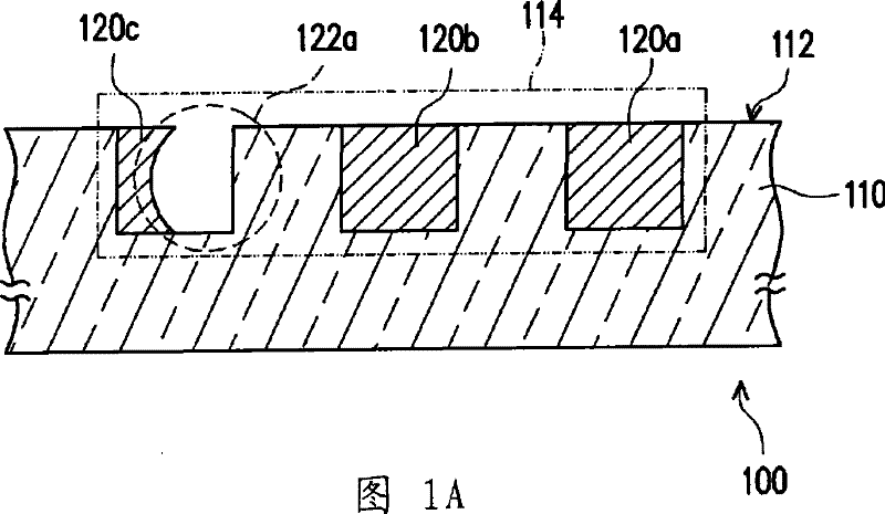
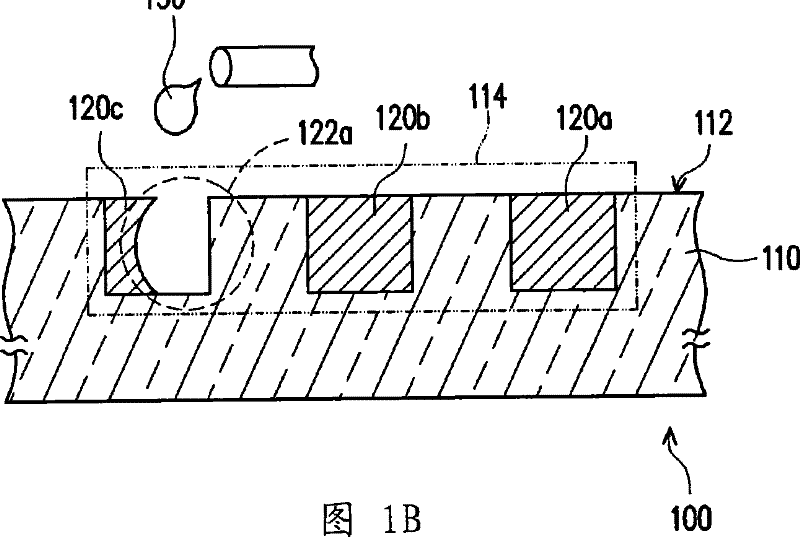
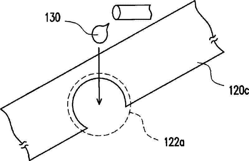
[0038] Figure 1A to Figure 1B It is a schematic cross-sectional view of a method for repairing circuits of an embedded circuit board according to an embodiment of the present invention, Figure 1C for repair Figure 1B The top view enlarged schematic diagram of the local circuit of the embedded circuit board. Please refer to Figure 1A According to the method for repairing the circuit of an embedded circuit board in this embodiment, firstly, an embedded circuit board 100 is provided. The embedded circuit board 100 includes a dielectric layer 110 and a plurality of circuits 120a-120c ( Figure 1A Only three are schematically shown in ), wherein the dielectric layer 110 has a surface 112 and an indented pattern 114, the lines 120a-120c are located in the indented pattern 114 of the dielectric layer 110, and the line 120c has a defect 122a.

[0039] It is worth mentioning that the structure of the embedded circuit board 100 may only have a single circuit layer, or may have mu...


PUM


Abstract

A method for repairing circuits of an embedded circuit board. First, embedded circuit boards are provided. Embedded circuit boards include dielectric layers and multiple circuits. The dielectric layer has a surface and a concave pattern. The circuits are located in the concave pattern, and some of the circuits have at least one defect. Then, the conductive fluid material is sprayed on the defect by jet printing to repair the circuit.

Description

technical field [0001] The invention relates to a circuit repair method, and in particular to a circuit repair method of an embedded circuit board. Background technique [0002] Today's circuit board technology has developed from a common non-embedded circuit board to an embedded circuit board. In detail, the common non-embedded circuit board is characterized by its circuits protruding from the surface of the dielectric layer, while the embedded circuit board is characterized by its circuits embedded in the dielectric layer. [0003] A conventional process for wiring embedded circuit boards includes the following steps. Firstly, a substrate with a metal layer and a metal carrier is provided. Next, a photoresist layer is coated on the metal layer. Then, exposing and developing the photoresist layer to form a patterned photoresist layer. Then, an electroplating process is performed on the metal layer to form a circuit layer, wherein the circuit layer has a plurality of wir...

Claims


Application Information

Patent Timeline
Patent Type & Authority Patents(China)
IPC IPC(8): H05K3/22H05K3/10H05K1/09
Inventor 曾子章陈俊谦
Owner UNIMICRON TECH CORP
Why Eureka
Try Eureka