

Display substrate and methode of manufacturing the same
A display substrate and manufacturing method technology, applied in semiconductor/solid-state device manufacturing, optics, instruments, etc., can solve the problems of display substrate manufacturing process limitations, display substrate defects, etc., and prevent non-planar defects and step differences Effect
- Summary
- Abstract
- Description
- Claims
- Application Information
AI Technical Summary
Problems solved by technology
Method used
Image

Examples
Embodiment 1
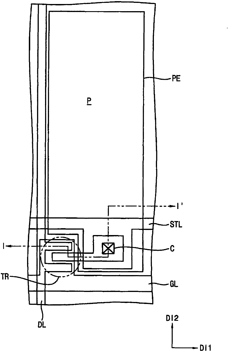
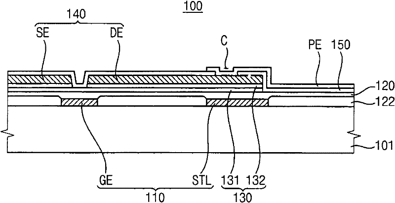
[0060] figure 1 is a top plan view showing a first exemplary embodiment of a display substrate 100 according to the present invention. figure 2 is along figure 1 A schematic cross-sectional view of the line I-I'.
[0061] refer to figure 1 and 2 , the display substrate 100 includes a base substrate 101 .
[0062] Gate line GL, gate electrode GE, storage line STL, planarization (planarization) layer 122, gate insulating layer 120, channel layer 130, data metal including data line DL, source electrode SE and drain electrode DE A layer 140 , a protective insulating layer 150 and a pixel electrode PE are formed on the base substrate 101 .
[0063] In the present exemplary embodiment, the gate line GL extends in the first direction D11. In one exemplary embodiment, the gate electrode GE may be connected to a portion of the gate line GL. Alternative exemplary embodiments include configurations in which the gate electrode GE may protrude from the gate line GL.
[0064] In th...
Embodiment 2
[0135] Figure 5 is a schematic cross-sectional view showing a second exemplary embodiment of a display substrate according to the present invention.
[0136] Figure 5 The top plan view of the shown display substrate is substantially similar to figure 1 The top plan view of the first exemplary embodiment of the display substrate is shown, therefore, its detailed description is omitted here.
[0137] also, Figure 5 The second exemplary embodiment of the shown display substrate is substantially similar to figure 2 The display substrate shown. therefore, Figure 5 The same reference numerals are used in the figure 2 Components that are the same as or similar to those shown in , and therefore, detailed descriptions thereof are omitted here.
[0138] refer to figure 2 and 5 , the display substrate 200 includes a base substrate 101 .
[0139] Gate line GL, gate electrode GE, storage line STL, planarization layer 122, gate insulating layer 120, channel layer 130, data ...
Embodiment 3
[0151] Figure 7 is a schematic cross-sectional view showing a display substrate according to a third exemplary embodiment of the present invention.
[0152] Figure 7 The plan view of the third exemplary embodiment of the display substrate shown in figure 1 The illustrated plan views of the first exemplary embodiment of the display substrate are substantially the same, and thus, detailed descriptions thereof are omitted.
[0153] In addition, in addition to including the deformation preventing layer 310, Figure 7 The third exemplary embodiment of the display substrate shown in figure 2 The display substrates shown in are basically the same. Thus, in Figure 7 use the same reference numerals in the figure 2 Components that are the same as or similar to those shown in , and therefore, detailed descriptions thereof are omitted.
[0154] refer to figure 2 and Figure 7 , the display substrate 300 includes a base substrate 101 .
[0155] Deformation prevention layer ...
PUM
| Property | Measurement | Unit |
|---|---|---|
| thickness | aaaaa | aaaaa |
| thickness | aaaaa | aaaaa |
| thickness | aaaaa | aaaaa |
Abstract
Description
Claims
Application Information