

Low internal stress copper electroplating method
A technology of copper ions and current density, applied in the direction of electrolytic components, electrolytic process, cells, etc., can solve the problems of reducing the efficiency and instability of the electroplating process
- Summary
- Abstract
- Description
- Claims
- Application Information
AI Technical Summary
Problems solved by technology
Method used
Image

Examples
Embodiment 1
[0047] The following table lists the composition and content of four aqueous acidic copper plating baths.
[0048]
[0049]
[0050] 1 PolyMax TM PA-66 / LC (available from Heritage Plastics, Inc. Picayune, MS, USA)
[0051] 2 PEG12000
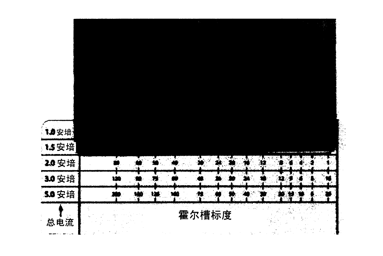
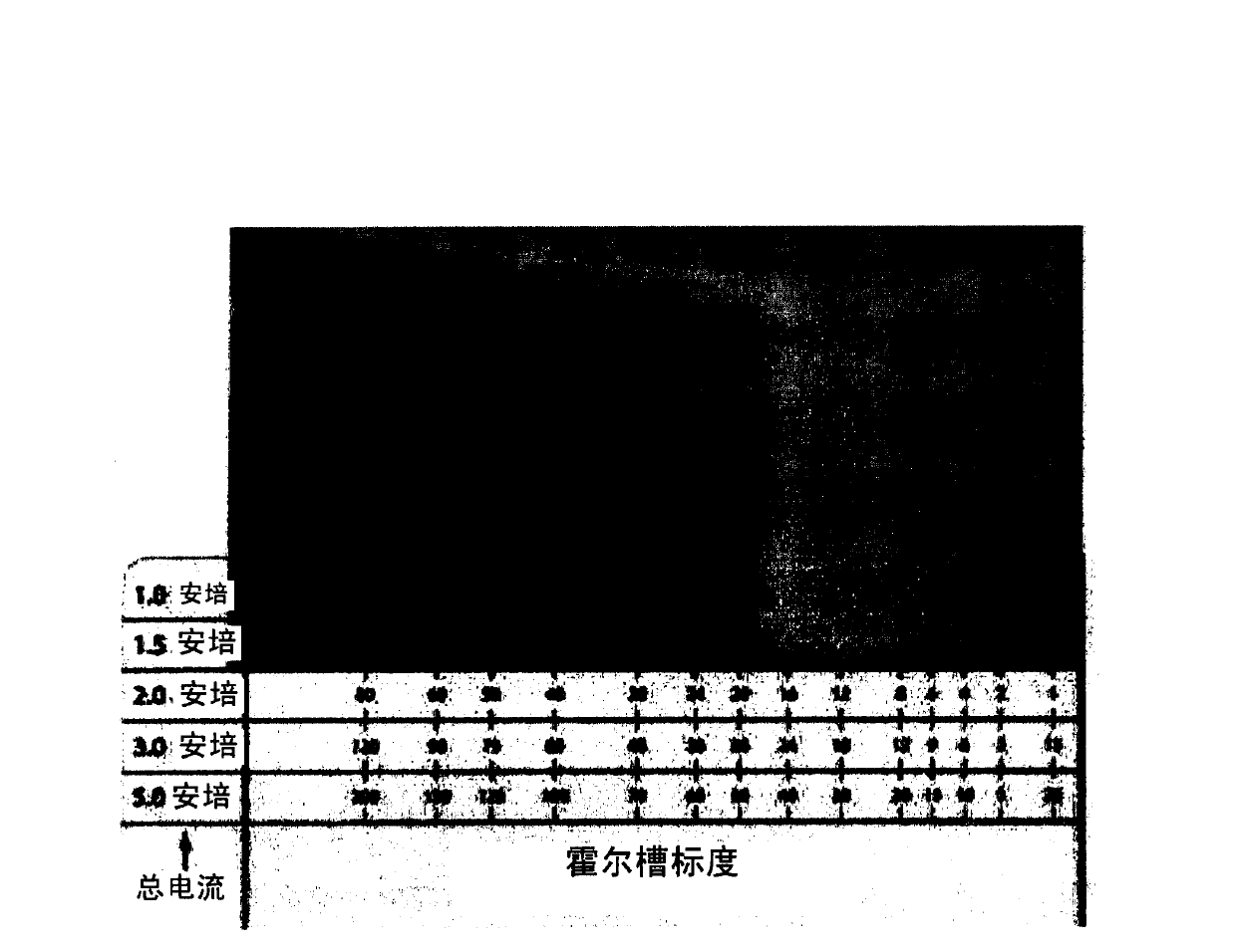
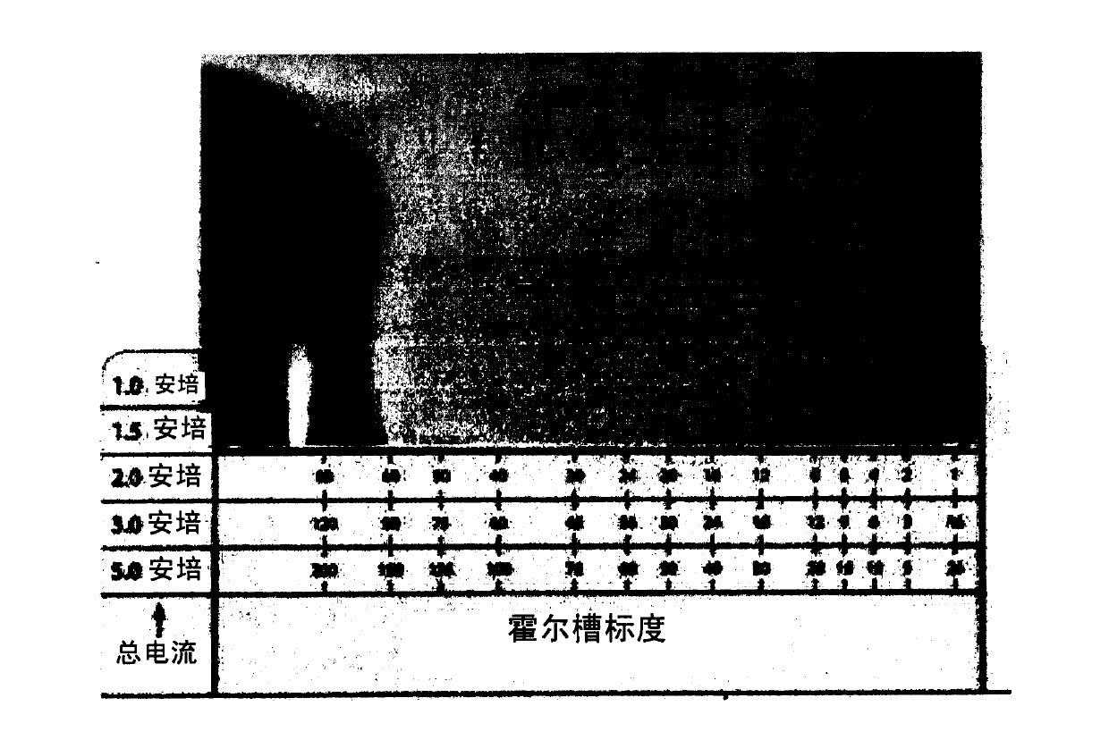
[0052] Each plating bath was placed in a conventional Hall cell equipped with a device capable of bubbling air at the test piece (cathode) area. The anode is metallic copper. The test piece is a conventional polished brass Hall slot. Each Hall cell test piece was cleaned until there was no trace of water film on the surface, and then moved to a Hall cell containing any one of the above four copper plating baths. The test piece and copper anode are connected to a rectifier so that the test piece, copper plating bath and anode form an electrical circuit. A total current density of 2 amps was applied to each test piece. Each test piece was plated for 10 minutes at a bath temperature of 30°C.
[0053] The plated copper-plated test pi...
Embodiment 2
[0056] Two flexible copper / beryllium foil test strips enable single-sided plating on the uncoated side by coating one side with a dielectric. Use plated tape to secure the test strips to the support substrate, see attached figure 2 , and the test strips were placed in a Harlem cell containing an acidic copper electroplating bath as in Bath 1 in the Table of Example 1. The temperature of the plating bath was room temperature. A metal copper strip is used as the anode. The test chaff and anode are connected to the rectifier. Copper electroplating was performed on the uncoated side of each test strip at an average current density of 50 ASF to obtain deposits with a thickness of 40-50 μm.
[0057] After plating is complete, remove the test strips from the Harlem cell, rinse with water, dry and remove the plated strips from the test strips. The copper deposits on each test strip were shiny. Due to the build-up of internal stresses in the copper deposit, each test strip exhibi...
Embodiment 3
[0059]Two flexible copper / beryllium foil test strips with dielectric coated on one side were electroplated with copper using the plating bath and method as described in Example 2 above. After plating, remove the test strips and support substrate from the Haring cell, rinse with water and dry. Copper deposits on the test strip are shiny. Remove the test strip from the support substrate and insert one end into a sediment stress analyzer (available from Specialty Testing and Development Co., Jacobus, PA, USA, www. .specialtytest.com) in screw grips. Test strips are at room temperature. The test strip bends and deforms within 4 hours, see attached Figure 3a . The internal stress of the copper deposits on both test bars was 160 psi. Internal stress is determined using the formula S=U / 3T×K, where S is the stress in psi, U is the deflection value from a calibrated scale, T is the deposit thickness in inches, and K is the calibration constant for the test strip . After aging e...
PUM
| Property | Measurement | Unit |
|---|---|---|
| Thickness | aaaaa | aaaaa |
Abstract
Description
Claims
Application Information