Composite substrate, method of manufacturing the same, a thin film device, and method of manufacturing the same

a technology of composite substrates and thin films, applied in the direction of printed circuits, inductances, stress/warp reduction, etc., can solve the problems of difficult to fabricate thin film devices stably, and become impossible to use electrolytic plating methods in forming conductive films

Inactive Publication Date: 2006-10-05
TDK CORPARATION
View PDF0 Cites 39 Cited by
  • Summary
  • Abstract
  • Description
  • Claims
  • Application Information

AI Technical Summary

Benefits of technology

[0027] According to the composite substrate of the present invention or its manufacturing method, in the case where the substrate and the conductive film thereon which has a laminated structure are provided, the conductive film is formed so that it may include a first conductive film with a tensile stress and a second conductive film with a compressive stress. As a result, the tensile stress of the first conductive film is offset by use of the compressive stress of the second conductive film. In this manner, deformation of the substrate in response to the influence of the internal stress of ...

Problems solved by technology

Therefore, there lay a problem that it is difficult to fabricate a thin film device stably.
But use of those series of conventional technique may cause a new problem while the problem of deformation of substrates is solved.
Besides, in the case where a conductive film is formed separately in ...

Method used


Image

  • Composite substrate, method of manufacturing the same, a thin film device, and method of manufacturing the same
  • Composite substrate, method of manufacturing the same, a thin film device, and method of manufacturing the same
  • Composite substrate, method of manufacturing the same, a thin film device, and method of manufacturing the same

Examples


Embodiment Construction

[0052] The present invention will now be described in detail with reference to the drawings showing preferred embodiments thereof.

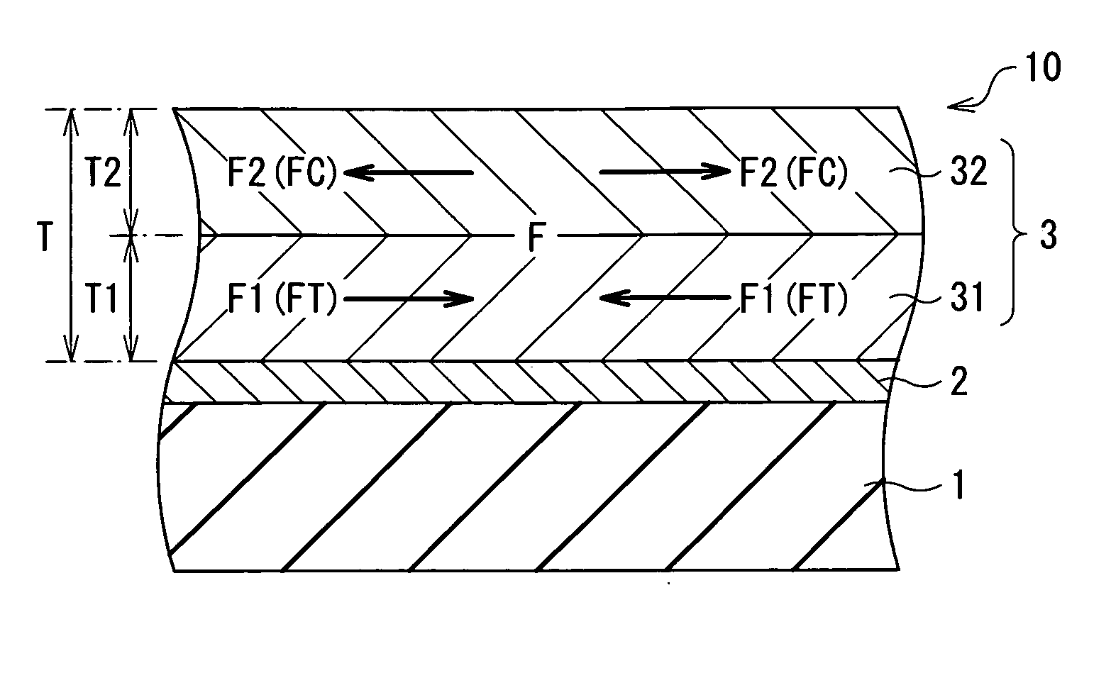
[0053] First, a composite substrate structure of one embodiment in the present invention will be described with reference to FIG. 1. FIG. 1 expresses a cross sectional configuration of a composite substrate 10.

[0054] The composite substrate 10 according to the embodiment is used in the thin film device field for various applications and, for example, applied to a thin film inductor, a thin film transformer, a thin film sensor, thin film resistance, a thin film actuator, a thin film magnetic head or MEMS (micro electro mechanical systems). The composite substrate 10 has a configuration that a conductive film 3 is formed on a substrate 1 as shown in FIG. 1. More specifically, the composite substrate 10 has a configuration that the conductive film 3 is formed on the substrate 1 via a seed film 2, namely, the seed film 2 and the conductive film 3 have been ...


PUM

PropertyMeasurementUnit
Electrical conductoraaaaaaaaaa
Stress optical coefficientaaaaaaaaaa
Deformation enthalpyaaaaaaaaaa

Abstract

A composite substrate capable of suppressing a deformation of the substrate in response to the influence of internal stress of a conductive film is provided. When a conductive film is formed on a substrate, the conductive film is formed so as to have a laminated structure including a main conductive film which has a tensile stress FT as its internal stress F1 and a sub-conductive film which has a compressive stress FC as its internal stress F2. In this manner, the tensile stress FT of the main conductive film is offset by use of the compressive stress FC of the sub-conductive film. Thereby, unlike the case where the conductive film is formed so that only the main conductive film may be included without including the sub-conductive film, the substrate becomes less deformable in response to the influence of the internal stress F of the conductive film.

Description

BACKGROUND OF THE INVENTION [0001] 1. Field of the Invention [0002] The present invention relates to a composite substrate including a substrate and a conductive film thereon, its manufacturing method, a thin film device to which the composite substrate is applied, and its manufacturing method. [0003] 2. Description of the Related Art [0004] Composite structure objects (what is called a composite substrate) with a substrate and a conductive film thereon have been used widely in the thin film device field of a various application in recent years. One example of such thin film devices using the composite substrate includes a thin film inductor provided with a coil that works as the above-mentioned conductive film. This thin film inductor basically has a structure where the coil is provided on a supporting substrate. [0005] In order to reduce the direct current resistance of the conductive film as for this composite substrate, it is requested that the thickness of the conductive film b...

Claims


Application Information

Patent Timeline
IPC IPC(8): B32B1/00B32B15/00
CPCH01F17/0006H01F2017/0046H01F2017/0066H05K1/0271Y10T428/24628H05K2201/0317H05K2201/0338Y10T428/32H05K1/09Y10T428/31678
Inventor MASAI, TAKU
Owner TDK CORPARATION
Why Eureka
Try Eureka