Supercharge Your Innovation With Domain-Expert AI Agents!

Charge pump

A charge pump and voltage technology, applied in circuits, electrical components, output power conversion devices, etc., can solve the problems affecting the efficiency of charge pumps, and achieve the effect of improving the "body effect" or leakage phenomenon and improving efficiency.

Active Publication Date: 2010-07-07
SEMICON MFG INT (SHANGHAI) CORP +1
View PDF0 Cites 9 Cited by
  • Summary
  • Abstract
  • Description
  • Claims
  • Application Information

AI Technical Summary

Problems solved by technology

Therefore, it will also affect the efficiency of the charge pump

Method used


Image

  • Charge pump
  • Charge pump
  • Charge pump

Examples


Embodiment approach

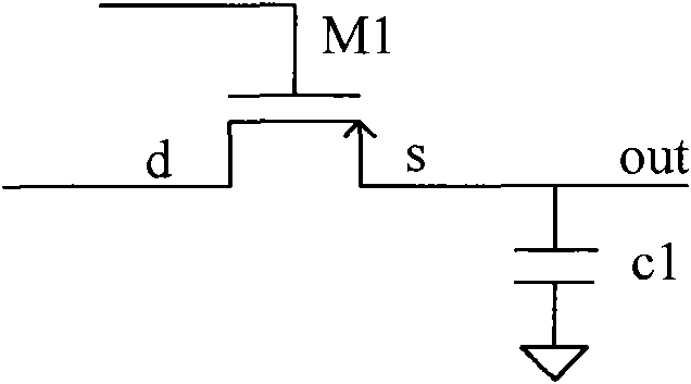
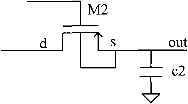
[0020] Based on this, according to an embodiment of the present invention, the charge pump may include:

[0021] a first boost circuit, configured to boost the power supply voltage;

[0022] The output MOS transistor coupled to the first boost circuit, which includes: a first input terminal, a first output terminal, a substrate terminal and a first control terminal, and the voltage of the substrate terminal is the first input terminal or the first output terminal The higher voltage in the terminal, the output MOS transistor is turned on under the control signal obtained by the control terminal, and the output voltage of the charge pump is formed according to the output voltage of the first boost circuit obtained by the first input terminal, and through output at the first output terminal.

[0023] In the above implementation manner, after the first boost circuit boosts the power supply voltage, the boosted voltage is output through the output MOS transistor. The voltage at t...


PUM


Abstract

The invention discloses a charge pump, comprising a first booster circuit for boosting the power supply voltage, and an output MOS tube coupled to the first booster circuit. The output MOS tube comprises a first input end, a first output end, a substrate end and a first control end, wherein the voltage of the substrate end is the higher voltage of the first input end or the first output end; the control end receives the control signal; the first input end is connected with the output of the first booster circuit, and the first output end is used as the output of the charge pump. The charge pump can improve the bulk effect and the electric current leakage.

Description

technical field [0001] The invention relates to the field of integrated circuit design, in particular to a charge pump. Background technique [0002] In current applications of non-volatile memories, high voltages are usually applied. These high voltages are typically provided by charge pumps. [0003] Figure 1a It is a partial circuit schematic diagram of a current charge pump. refer to Figure 1a As shown, the circuit includes a PMOS transistor M1 and a capacitor C1 connected to the source (s) of the PMOS transistor, and the source of the PMOS transistor is used as the output (out) of the charge pump. By controlling the gate voltage of the PMOS transistor M1 to turn it on, so that the current at the drain (d) is transmitted to the capacitor C1 to charge the capacitor C1. Through charging, the charge on the capacitor C1 gradually accumulates, so that the source voltage of the PMOS transistor M1 increases. However, when the source voltage of the PMOS transistor M1 rises...

Claims


Application Information

Patent Timeline
Patent Type & Authority Applications(China)
IPC IPC(8): H02M3/07
CPCH02M3/07H02M2003/078H03K17/063H03K2217/0018Y10T29/49002H02M3/078
Inventor 刘志纲俞大立
Owner SEMICON MFG INT (SHANGHAI) CORP
Features
  • R&D
  • Intellectual Property
  • Life Sciences
  • Materials
  • Tech Scout
  • Unparalleled Data Quality
  • Higher Quality Content
  • 60% Fewer Hallucinations
Learn More