Local interconnect structure for a CMOS image sensor and its manufacturing method

A local interconnection and pixel technology, which is applied in the fields of semiconductor/solid-state device components, semiconductor devices, electric solid-state devices, etc., can solve the problems of low cost, high performance, and difficulty in laying access and output signal lines and power lines, etc. Achieve the effect of improving wiring accuracy, simplifying wiring process, improving optical crosstalk and microscope head capability

Active Publication Date: 2010-07-14
OMNIVISION TECH INC
View PDF0 Cites 0 Cited by
  • Summary
  • Abstract
  • Description
  • Claims
  • Application Information

AI Technical Summary

Problems solved by technology

In addition, the speed of obtaining and reading data is also an issue
Smaller, more complex pixels make it difficult to route all the signal and power lines to and from the pixel array while maintaining low cost and high performance
To further complicate matters, the "stack height" of the image sensor is also a factor

Method used


Image

  • Local interconnect structure for a CMOS image sensor and its manufacturing method
  • Local interconnect structure for a CMOS image sensor and its manufacturing method
  • Local interconnect structure for a CMOS image sensor and its manufacturing method

Examples


Embodiment Construction

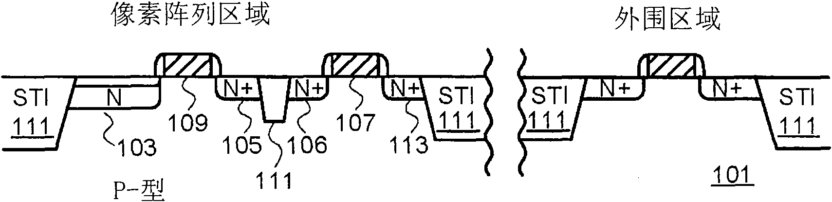
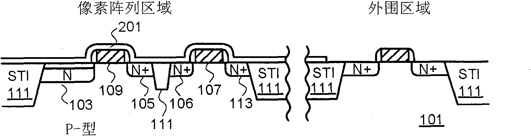
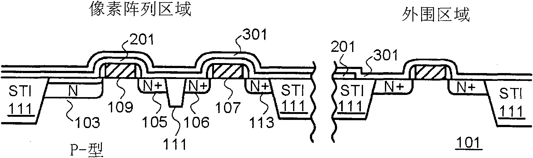
[0023] In the following description, numerous specific details are provided in order to provide a thorough understanding of embodiments of the invention. One skilled in the art will recognize, however, that the invention can be practiced without one or more of these specific details, or that the invention can be practiced with other methods, elements, etc. In addition, well-known structures and operations are not shown or described in detail in order to clearly describe the various embodiments of the present invention.

[0024] In the description of the present invention, when referring to "an embodiment" or "a certain embodiment", it means that the specific features, structures or characteristics described in this embodiment are included in at least one embodiment of the present invention. Thus, appearances of "in an embodiment" or "in a certain embodiment" in various places in the specification do not necessarily refer to all belonging to the same embodiment; manner combine...


PUM


Abstract

The invention provides a local interconnect structure for a CMOS image sensor and its manufacturing method. A self-aligned silicide (salicide) process is used to form a local interconnect for a CMOS image sensor consistent with a conventional CMOS image sensor process flow. An oxide layer is deposited over the pixel array of the image sensor. Portions of the oxide layer is removed and a metal layer is deposited. The metal layer is annealed to form a metal silicide. Optionally, a protective insulation layer is then deposited.

Description

[0001] Divisional statement [0002] This application is a divisional application of a Chinese patent application filed on December 8, 2005 with application number 200510130905.1 and the title of the invention is "Local interconnection structure of CMOS image sensor and method for forming it"; and claims US patent application 11 / 007,859 This application was filed on December 9, 2004 as a priority. technical field [0003] The present invention relates to image sensors, and more particularly, the present invention relates to an image sensor including a local interconnect structure. Background technique [0004] Image sensors have become ubiquitous, and they are widely used in digital cameras, cellular phones, security cameras, medical equipment, automobiles, and other applications. The technology of manufacturing image sensors, especially CMOS (Complementary Metal Oxide Semiconductor) image sensors continues to develop rapidly. For example, the requirements of high resoluti...

Claims


Application Information

Patent Timeline
Patent Type & Authority Applications(China)
IPC IPC(8): H01L21/768H01L27/146H01L23/528
CPCH01L27/14636H01L27/14643H01L27/14689H01L21/76895H01L27/14601
Inventor 霍华德·E·罗德斯
Owner OMNIVISION TECH INC
Why Eureka
Try Eureka