Manufacturing method of split-gate type flash memory of shared word line

A split-gate flash memory and manufacturing method technology, which is applied in semiconductor/solid-state device manufacturing, electrical components, circuits, etc., can solve the problem of device programming voltage reduction, reduce erasing voltage, reduce area, and avoid over-erasing Effect

Active Publication Date: 2010-07-14
SHANGHAI HUAHONG GRACE SEMICON MFG CORP
View PDF3 Cites 17 Cited by
  • Summary
  • Abstract
  • Description
  • Claims
  • Application Information

AI Technical Summary

Problems solved by technology

When traditional flash memory is moving towards higher storage density, due to structural limitations, it will face great challenges to further reduce the programming voltage of the device

Method used


Image

  • Manufacturing method of split-gate type flash memory of shared word line
  • Manufacturing method of split-gate type flash memory of shared word line
  • Manufacturing method of split-gate type flash memory of shared word line

Examples


Embodiment Construction

[0033] In order to better understand the technical content of the present invention, specific embodiments are given together with the attached drawings for description as follows.

[0034] The present invention proposes a split-gate flash memory manufacturing method that shares word lines, which can effectively reduce the area of ​​the chip while keeping the electrical isolation performance of the chip unchanged, and can also reduce the erasing voltage to avoid over-erasing The problem.

[0035] Please refer to figure 1 , figure 1 Shown is a flow chart of a method for manufacturing a split-gate flash memory sharing a word line according to a preferred embodiment of the present invention. The present invention proposes a method for manufacturing a split-gate flash memory that shares a word line, comprising the following steps:

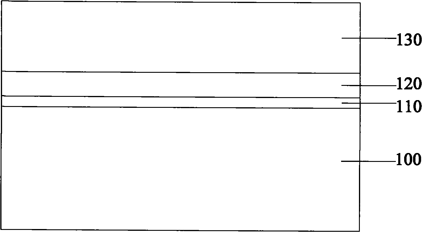
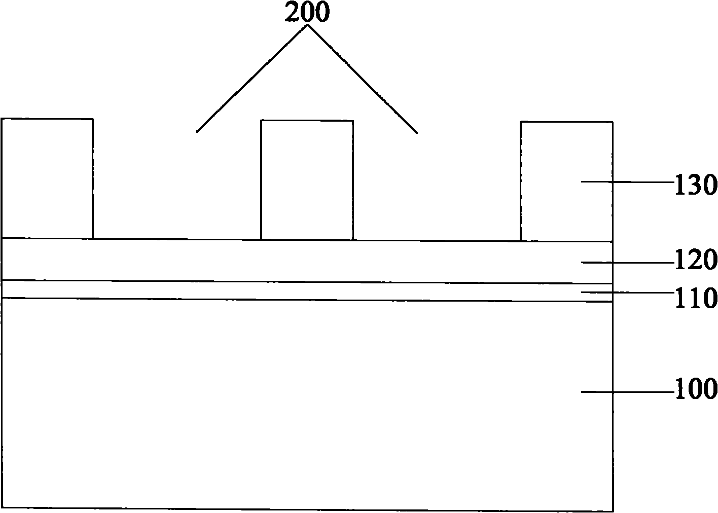
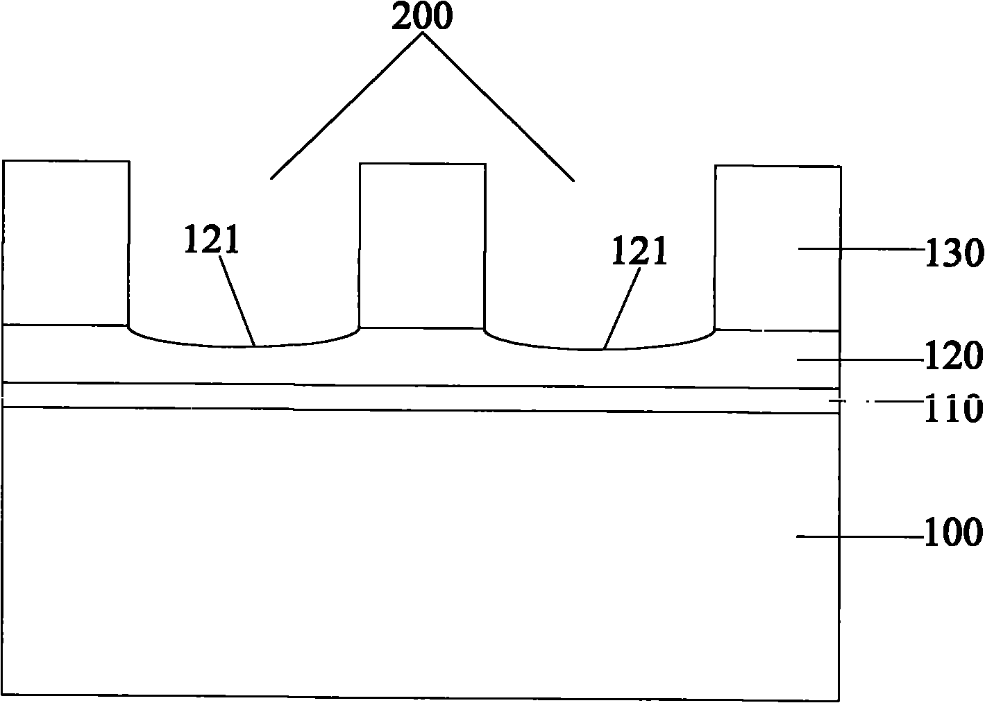
[0036] Such as figure 1 As shown in , the present invention provides a semiconductor substrate 100, and sequentially deposits a silicon dioxide ...


PUM


Abstract

The invention provides manufacturing method of a split-gate type flash memory of a shared word line. The split-gate type flash memory of the obtained shared word line enables two memory bit units to share one word line, realizes the read, programming and the erasure of the memory bit units by applying different working voltages to the word line, two control gates and a source drain area, can effectively reduce the area of a small chip under the condition of keeping the electric isolation of the chip unchanged due to a shared bit line structure and also prevent the problem of erasure and is beneficial to strengthening a tunnelling electric field when a device is erased due to a self-aligned structure formed by a floating gate positioned on a top end and the work line, thereby effectively reducing the erasure voltage.

Description

technical field [0001] The invention relates to the field of semiconductor design and manufacture, and in particular to a method for manufacturing split-gate flash memory with shared word lines. Background technique [0002] Flash memory has become a research hotspot in non-volatile memory due to its convenience, high storage density, and good reliability. Since the first flash memory product came out in the 1980s, with the development of technology and the storage needs of various electronic products, flash memory has been widely used in mobile and communication devices such as mobile phones, notebooks, handheld computers and U disks. , flash memory is a kind of non-volatile memory. Its operating principle is to control the switch of the gate channel by changing the critical voltage of the transistor or memory cell to achieve the purpose of storing data, so that the data stored in the memory will not be lost due to power interruption. Disappears, and flash memory is a spec...

Claims


Application Information

Patent Timeline
Patent Type & Authority Applications(China)
IPC IPC(8): H01L21/8247
Inventor 曹子贵
Owner SHANGHAI HUAHONG GRACE SEMICON MFG CORP
Why Eureka
Try Eureka