Method for manufacturing word-line-sharing noncontact split-grid flash memory

A split-gate flash memory and manufacturing method technology, which is applied in semiconductor/solid-state device manufacturing, electrical components, circuits, etc., can solve the problem of device programming voltage reduction, and achieve the effect of device size reduction, small size, and reduced area

Active Publication Date: 2014-03-19
SHANGHAI HUAHONG GRACE SEMICON MFG CORP
View PDF5 Cites 0 Cited by
  • Summary
  • Abstract
  • Description
  • Claims
  • Application Information

AI Technical Summary

Problems solved by technology

When traditional flash memory is moving towards higher storage density, due to structural limitations, it will face great challenges to further reduce the programming voltage of the device

Method used


Image

  • Method for manufacturing word-line-sharing noncontact split-grid flash memory
  • Method for manufacturing word-line-sharing noncontact split-grid flash memory
  • Method for manufacturing word-line-sharing noncontact split-grid flash memory

Examples


Embodiment Construction

[0035] In order to better understand the technical content of the present invention, specific embodiments are given together with the attached drawings for description as follows.

[0036] The present invention proposes a non-contact split-gate flash memory manufacturing method for sharing word lines. The obtained flash memory device can effectively reduce the area of ​​the chip while keeping the electrical isolation performance of the chip unchanged, and at the same time avoid excessive The problem of erasing.

[0037] The present invention proposes a method for manufacturing a non-contact split-gate flash memory sharing a word line, which includes the following steps:

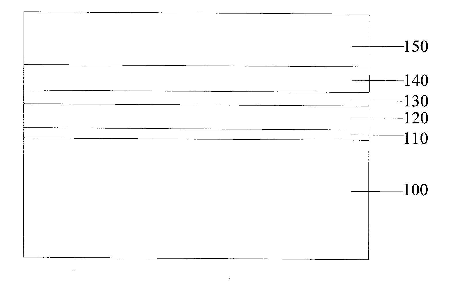
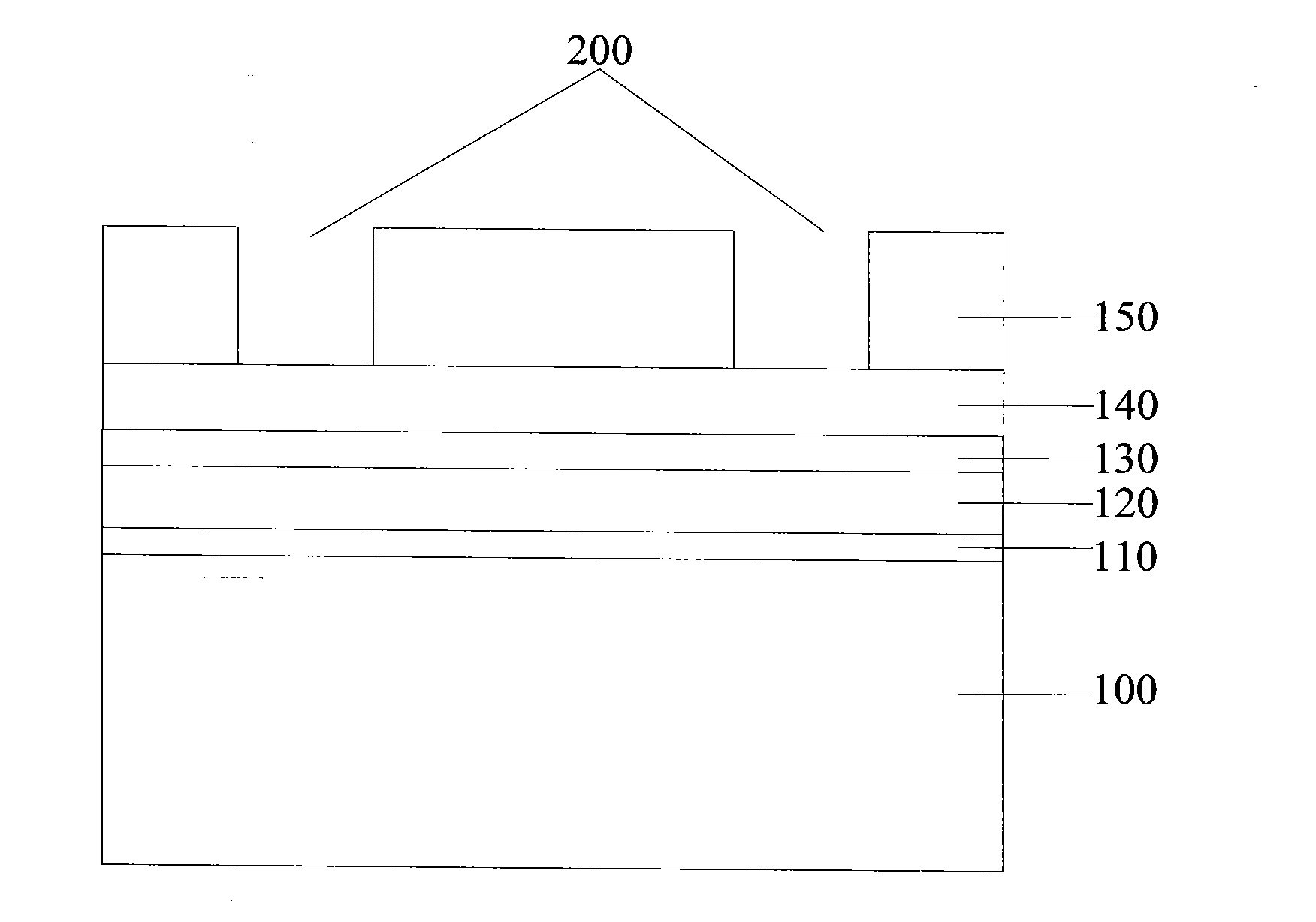
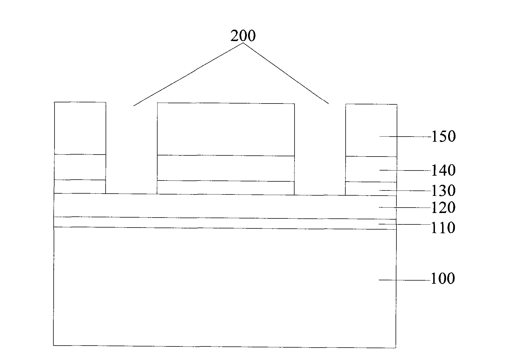
[0038] Please refer to figure 1 , the present invention provides a semiconductor substrate 100, and sequentially deposits a first oxide layer 110, a floating gate polysilicon layer 120, a second oxide layer 130, a control gate polysilicon layer 140 and a silicon nitride layer 150; wherein, the first oxide ...


PUM


Abstract

The invention provides a method for manufacturing a word-line-sharing noncontact split-grid flash memory. Two storage units share one word line, and the reading, programming and erasing of the storage units are realized by applying different working voltages to the word line, a first control grid, a second control grid, a first bit line and a second bit line; the structure of sharing bit line can effectively reduce the area of a chip under the condition that the split-grid flash memory can keep the electrical isolation property unchanged, and simultaneously avoid the problem of over erasing. Meanwhile, due to the adoption of the noncontact design, the flash memory device has the characteristics of small size and compatibility of the process with the CMOS (Complementary Metal Oxide Semiconductor) traditional process, thereby being benefit to the further reduction of the size of the device.

Description

technical field [0001] The invention relates to the field of semiconductor design and manufacture, and in particular to a method for manufacturing a non-contact split-gate flash memory sharing a word line. Background technique [0002] Flash memory has become a research hotspot in non-volatile memory due to its convenience, high storage density, and good reliability. Since the first flash memory product came out in the 1980s, with the development of technology and the storage needs of various electronic products, flash memory has been widely used in mobile and communication devices such as mobile phones, notebooks, handheld computers and U disks. , flash memory is a kind of non-volatile memory. Its operating principle is to control the switch of the gate channel by changing the critical voltage of the transistor or memory cell to achieve the purpose of storing data, so that the data stored in the memory will not be lost due to power interruption. Disappears, and flash memor...

Claims


Application Information

Patent Timeline
Patent Type & Authority Patents(China)
IPC IPC(8): H01L21/8247
Inventor 曹子贵
Owner SHANGHAI HUAHONG GRACE SEMICON MFG CORP
Why Eureka
Try Eureka