Non-contact nano-crystalline split-gate flash memory for sharing word line
A split-gate flash memory and nanocrystalline technology, which is applied in the direction of electrical components, electrical solid devices, circuits, etc., can solve the problem of device programming voltage reduction, achieve device size reduction, reduce area, and avoid over-erasing effects
- Summary
- Abstract
- Description
- Claims
- Application Information
AI Technical Summary
Problems solved by technology
Method used
Image
Examples
Embodiment Construction
[0026] In order to better understand the technical content of the present invention, specific embodiments are given together with the attached drawings for description as follows.
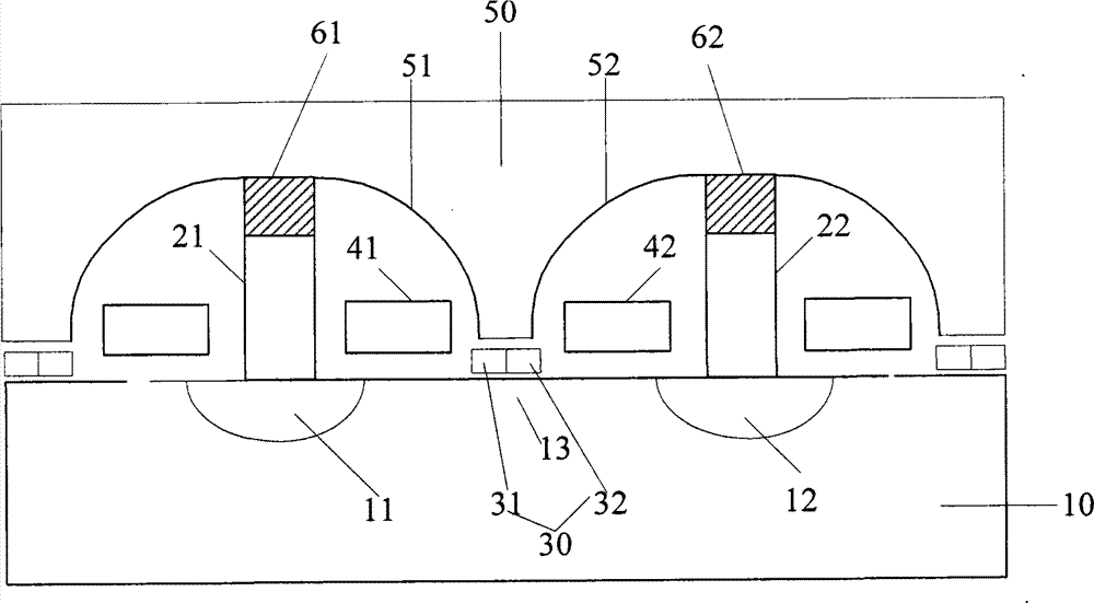
[0027] The present invention proposes a non-contact nanocrystalline split-gate flash memory that shares word lines. The obtained flash memory device can effectively reduce the area of the chip while keeping the electrical isolation performance of the chip unchanged, and at the same time avoid excessive The problem of erasing.
[0028] Please refer to figure 1 , figure 1 Shown is a schematic diagram of the structure of a non-contact nanocrystalline split-gate flash memory sharing a word line according to a preferred embodiment of the present invention. The present invention proposes a non-contact nanocrystalline split-gate flash memory sharing a word line, comprising: a semiconductor substrate 10 having source regions 11 and drain regions 12 arranged at intervals thereon; a channel region 13 loc...
PUM
 Abstract
Description
Claims
Application Information
