Pixel structure and electroluminescence device

A technology of electroluminescence device and pixel structure, which is applied to circuits, electrical components, electric solid devices, etc., can solve the problems of poor uniformity of light emission of light-emitting devices, and achieve the effect of reducing the equivalent resistance value

Active Publication Date: 2012-01-25
AU OPTRONICS CORP
View PDF0 Cites 0 Cited by
  • Summary
  • Abstract
  • Description
  • Claims
  • Application Information

AI Technical Summary

Problems solved by technology

Therefore, the overall luminous uniformity of the electroluminescent device will be poor

Method used


Image

  • Pixel structure and electroluminescence device
  • Pixel structure and electroluminescence device
  • Pixel structure and electroluminescence device

Examples


Embodiment Construction

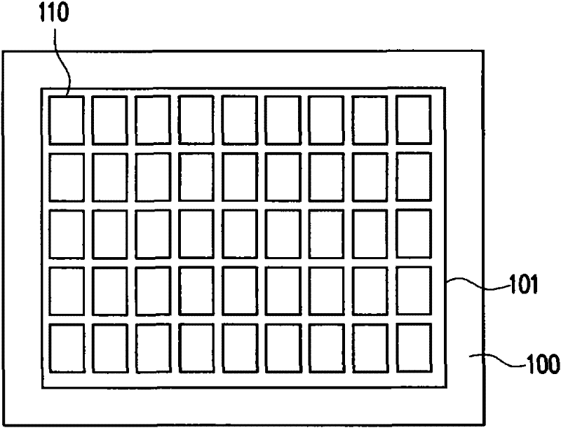
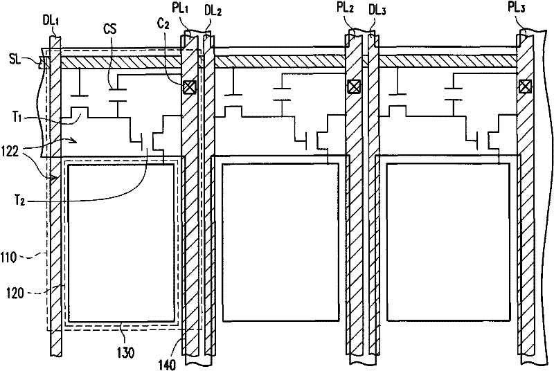
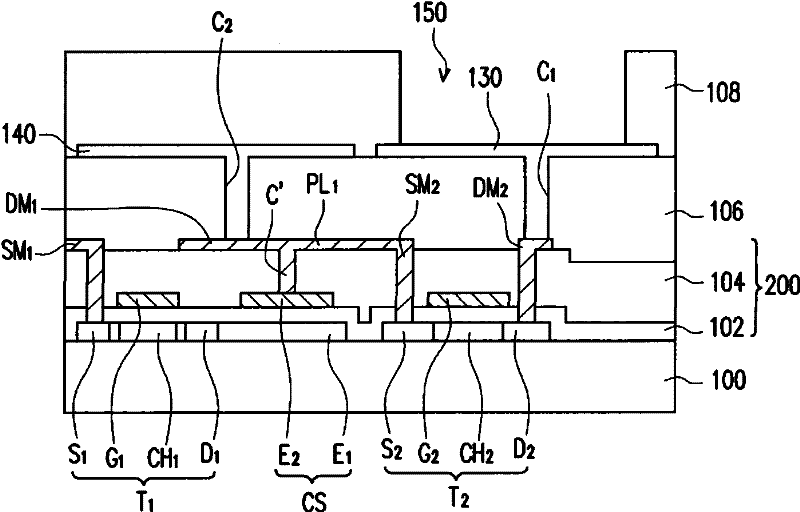
[0050] figure 1 is a schematic top view of an electroluminescent device according to an embodiment of the present invention. figure 2 yes figure 1 A partial schematic diagram of a pixel array in an electroluminescent device. Figure 3A is a schematic partial cross-sectional view of one of the pixel structures according to an embodiment of the present invention. To elaborate, figure 2 as well as Figure 3A The pixel structure shown does not show the light emitting layer and the second electrode layer of the light emitting element. A cross-section of the complete pixel structure is depicted in Figure 3B middle.

[0051] Please refer to figure 1 as well as figure 2 , the electroluminescent device of this embodiment has a display area 101, and the display area 101 has a plurality of pixel areas 110, and a pixel structure is disposed in each pixel area 110 to form a pixel array. Since the area around the display area 101 is not used for display, it can also be called a...


PUM


Abstract

The invention relates to a pixel structure which is located in a display zone which is provided with a luminous zone and a non-luminous zone; wherein the pixel structure of a electroluminescence device comprises a first active component, a second active component, a light-emitting component and an auxiliary electrode layer. The first active component is electrically connected with a scanning lineand a data line. The second active component is electrically connected with the first active component and a power line. The light-emitting component is located in the luminous zone and is electrically connected with the second active component; in addition, the light-emitting component comprises a first electrode layer which is electrically connected with the second active component, a luminous layer located on the first electrode layer and a scone electrode layer located on the luminous layer. The auxiliary electrode layer is electrically connected with the power line.

Description

technical field [0001] The present invention relates to a pixel structure, and in particular to a pixel structure of an electroluminescent device and an electroluminescent device having the pixel structure. Background technique [0002] An electroluminescent device is a self-luminous (Emissive) device. Because the electroluminescent device has no viewing angle limitation, low manufacturing cost, high response speed, power saving, DC drive that can be used in portable machines, wide operating temperature range and light weight, it can be miniaturized and thinned with hardware equipment, etc. . Therefore, the electroluminescent device has great development potential and is expected to become a novel flat panel display of the next generation. [0003] Generally speaking, an electroluminescent device is composed of an upper electrode layer, a lower electrode layer, and a light-emitting layer sandwiched between the two electrode layers. The lower electrode layer is generally ma...

Claims


Application Information

Patent Timeline
Patent Type & Authority Patents(China)
IPC IPC(8): H01L27/32H01L27/15H01L23/528
Inventor 周佳伶吴元均张立勋
Owner AU OPTRONICS CORP
Why Eureka
Try Eureka